
This is the accepted manuscript made available via CHORUS. The article has been
published as:
Direct Cation Exchange in Monolayer MoS_{2} via
Recombination-Enhanced Migration
Shi-Ze Yang, Weiwei Sun, Yu-Yang Zhang (张余洋), Yongji Gong, Mark P. Oxley, Andrew R.
Lupini, Pulickel M. Ajayan, Matthew F. Chisholm, Sokrates T. Pantelides, and Wu Zhou (周武)
Phys. Rev. Lett. 122, 106101 — Published 11 March 2019
DOI: 10.1103/PhysRevLett.122.106101

1
Direct cation exchange in monolayer MoS
2
via “explosive”
recombination-enhanced migration
Shi-Ze Yang
1, #
, Weiwei Sun
2,1,#
, Yu-Yang Zhang
3,2
, Yongji Gong
4
, Mark P. Oxley
1
,
Andrew R. Lupini
1
, Pulickel M. Ajayan
5
, Matthew F. Chisholm
1
,
Sokrates T.
Pantelides
2,3*
, Wu Zhou (周武)
3,1*
1
Center for Nanophase Materials Science, Oak Ridge National Laboratory, Oak
Ridge, Tennessee 37831, USA
2
Department of Physics and Astronomy and Department of Electrical Engineering
and Computer Science, Vanderbilt University, Nashville, Tennessee 37235, USA
3
School of Physical Sciences and CAS Center for Excellence in Topological Quantum
Computation, University of Chinese Academy of Sciences, Beijing 100049, China
4
School of Materials Science & Engineering, Beihang University, Beijing 100191,
China.
5
Department of Materials Science & NanoEngineering, Rice University, Houston,
Texas 77005, USA
# These authors contributed equally to this work.
*Corresponding authors: Sokrates T. Pantelides (pantelides@vanderbilt.edu
) or Wu
Zhou ([email protected]
)
Notice of Copyright:
This manuscript has been co-authored by UT-Battelle, LLC, under contract DE-AC05-00OR22725
with the US Department of Energy (DOE). The US government retains and the publisher, by
accepting the article for publication, acknowledges that the US government retains a nonexclusive,
paid-up, irrevocable, worldwide license to publish or reproduce the published form of this
manuscript, or allow others to do so, for US government purposes. DOE will provide public access
to these results of federally sponsored research in accordance with the DOE Public Access Plan
(http://energy.gov/downloads/doe-public-access-plan).
2
In addition to their unique optical and electronic properties, two-dimensional
materials provide opportunities to directly observe atomic-scale defect dynamics.
Here we use scanning transmission electron microscopy to observe substitutional
Re impurities in monolayer MoS
2
undergo direct exchanges with neighboring
Mo atoms in the lattice. Density-functional-theory calculations find that the
energy barrier for direct exchange, a process that has only been studied as a
diffusion mechanism in bulk materials, is too large for either thermal activation
or energy directly transferred from the electron beam. The presence of multiple S
vacancies next to the exchanged Re-Mo pair, as observed by electron microscopy,
does not lower the energy barrier sufficiently to account for the observed atomic
exchange. Instead, the calculations find that a Re dopant and surrounding S
vacancies introduce an ever-changing set of deep levels in the energy gap. We
propose that these levels mediate an “explosive” recombination-enhanced
migration via multiple electron-hole recombination events.
As a proof-of-concept,
we also show that Re-Mo direct exchange can be triggered via controlled creation
of sulfur-vacancies. The present experimental and theoretical findings lay a
fundamental framework towards manipulating single substitutional dopants in
two-dimensional materials.
Two-dimensional materials exhibit unique properties that can be used for novel
applications, but just as is the case with semiconductors, it is usually necessary to
introduce impurities to achieve desirable functionalization. “Defect engineering”
raises many challenges and holds many promises. It has been demonstrated that
aberration-corrected scanning transmission electron microscopy (STEM) provides
atomic-resolution images [1-6] that can be used to track impurity atoms in both two-
and three-dimensional materials and can directly monitor the defect reactions that
enable defect engineering. More recently, Lin et al. used the electron beam of a
STEM to sculpt and simultaneously image nanowires that are only three-atoms wide
in transition-metal dichalcogenide monolayers [7]. Ishikawa et al. reported the direct
observation of the migration of Ce and Mn dopant-atoms in a bulk AlN crystal [8].
3
Han et al. reported observations of migrating iridium adatoms and tri-iridium clusters
on MgO surfaces [9]. Susi et al. reported the observation of silicon dopants in
graphene undergoing beam-induced direct interchange with neighboring C atoms [10],
a key step towards the control of single dopant atoms [11,12]. All these investigations
show that STEM is a powerful tool for studying local atomic movements.
In general, thermal diffusion of substitutional impurities is mediated by native defects
such as vacancies and self-interstitials [13]. These processes are well understood and
are used widely to model dopant diffusion for engineering applications [14]. The
direct exchange between a substitutional impurity and a neighboring host atom has
been discussed in the literature going back to the 1940’s [15-18], but the energy
barrier for such a process is generally believed to be too large. In 1986, Pandey [18]
predicted that the energy barrier for direct exchange (he called it concerted exchange)
for self-diffusion in Si is comparable to the activation energy for self-diffusion
mediated by vacancies or self-interstitials, but verification of such prediction has been
lacking. In only one case, namely boron-doped copper, direct exchange was indirectly
established by ruling out defect-mediated mechanisms [19]. So far, the only
atomic-scale observation of direct exchange was the inversion of Si-C bonds in
graphene, first reported by Susi et al., where they describe a process induced by
momentum transferred from the incident electron beam [10]. However, it is likely that
other mechanisms also play a role for semiconducting materials.
In this Letter, we report the experimental observation of direct exchange between
substitutional Re and Mo host atoms in monolayer MoS
2
by monitoring Re atoms in
atomically-resolved STEM images. Density-functional theory (DFT) has been
employed to investigate several possible pathways for the direct exchange. We find
that the exchange barrier is initially very large (~11 eV), but it is lowered by
surrounding the cation with sulfur vacancies, which create extra space and weaken the
local bonding. However, even with six sulfur vacancies surrounding a Re atom, the
calculated exchange barrier is only reduced to ~2.4 eV. This value is still much higher
4
than the maximum energy, 1.45 eV, transferred to Mo atoms (or 0.75 eV transferred to
Re atoms) by the 60 kV electron beam for a single elastic collision and too high to
occur efficiently at room temperature. DFT calculations suggest an alternative
energy-transfer mechanism as follows. The hydrogenic level of an isolated
substitutional Re impurity becomes deeper and deeper with larger and larger
displacements of the Re atom. Moreover, when S vacancies are introduced, additional
deep levels appear in the energy gap, so that the gap contains several deep levels that
constantly move up and down and appear and disappear as S vacancies come and go.
These dynamic energy levels provide multiple paths for the recombination of
beam-generated electron-hole pairs. The energy released by these “explosive”
recombination events is transferred to local vibrations that ultimately enable the direct
exchange of Re dopants as observed in STEM. The required spectator S vacancies
make it possible to control the diffusion process through controlled creation of
sulfur-vacancies as we show in a proof-of-concept experimental demonstration.
The monolayer Re-doped MoS
2
sample used in our experiments was grown on a
SiO
2
/Si substrate using a chemical vapor deposition method with molybdenum oxide,
sulfur and ammonium perrhenate powders as Mo, S and Re sources, respectively [20].
The as-grown sample was transferred onto a TEM grid and the STEM imaging was
performed with an aberration-corrected scanning transmission electron microscope
operated at 60 kV using the medium angle annular dark field (MAADF, inner angle
50 mrad, outer angle 300 mrad) imaging mode with a beam current of about 9 pA (see
Methods in the Supplementary Information).
Electron microscopy characterization reveals that Re dopants are substitutional in the
MoS
2
lattice [20]. The intensity in MAADF images is roughly proportional to Z
2-x
,
where Z is the atomic number and x is a fractional number depending on the exact
experimental parameters [5]. The STEM images in Fig. 1 show that single Re atoms
occupy Mo sites in the hexagonal MoS
2
lattice and they appear as bright spots in the
MAADF image. Although double Mo atoms (i.e. a surface Mo adatom on top of a
5
lattice Mo atom) have similar MAADF image contrast as that from a substituted Re
atom, they can be easily identified in experiment as adsorbed Mo adatoms hop around
easily under electron beam irradiation [21]. The stable configurations of the bright
cation before and after direct exchange, therefore, rule out the possibility that these
features are due to surface Mo adatoms, and the good agreement between the
simulated image intensities with the experimental MAADF image verifies that the
brightest features in the experimental MAADF images are substitutional Re atoms
(Fig. 1).
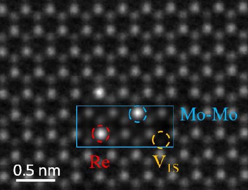
FIG 1. Comparison between experimental and simulated STEM-MAADF images.
The simulated MAADF image (indicated by the blue rectangle) is superimposed on
top of the experimental image. Substitutional Re site, double Mo column, and single S
vacancy (V
1S
) are highlighted by red, blue, and orange, respectively, in the simulated
image.
In addition to the observation of substitutional Re dopants in the MoS
2
lattice, a
Re-Mo exchange event is identified by analyzing the recorded sequential MAADF
images in areas where Re dopants are isolated. The exchange process is illustrated by
the different Re positions in the MAADF images recorded at time t
0
and t
0
+3.5 second
(s) as shown in Fig. 2, where the Re atom exchanged positions with a neighboring Mo

6
atom. In the images that document the exchange event (Figs. 2a and 2b), we observe
several S vacancies. The number and arrangements of S vacancies before and after the
exchange event are different. It is inferred that sulfur vacancies may play a role in the
Re-Mo exchange. The contribution of S vacancies will be further investigated using
theoretical calculations as described in the following paragraphs. Mo vacancies were
not observed during the cation exchange.
FIG 2. Direct Re-Mo exchange in Re-doped monolayer MoS
2
. (a, c)
STEM-MAADF images showing the position of the Re relative to other Re atoms (a)
and (c) the local area of Re doped MoS
2
with the corresponding structural model (e),
recorded at time t
0
before the exchange event. (b, d) STEM-MAADF images showing
the position of the Re relative to other Re atoms (b) and (d) the local MAADF image
with the corresponding structural model (f) recorded after the exchange event at
t
0
+3.5 seconds. The exchange of Re and Mo atoms is highlighted by blue and red
arrows, while sulfur mono-vacancies are indicated by orange dashed circles and sulfur
double-vacancies are indicated by yellow dashed circles. Re atoms are in red, Mo in
blue, and sulfur in yellow.
7
In order to elucidate the mechanism for the Re-Mo exchange process and the pertinent
activation energy, we performed systematic DFT calculations using the projector
augmented wave (PAW) method [22,23], as implemented in the Vienna Ab-initio
Simulation Package (VASP) [24-26]. Total energies were obtained in the generalized
gradient approximation (GGA) using the PBE functional formulated by Perdew,
Burke, and Ernzerhof [27]. For Mo, S, and Re atoms, Mo-4p, 4d, and 5s; S-3s, and 3p;
and Re-5p, 5d, and 5s states were treated as valence states. A cutoff energy of 500 eV
was used in all calculations. We used a 7×7 supercell with a 2×2×1 Monkhorst-Pack
k-point mesh. The Re-Mo exchange barrier was calculated in the presence of different
numbers of sulfur vacancies.
To determine migration barriers, we used the nudged elastic band (NEB) method
implemented within density-functional theory. In the calculations, three migration
pathways (see Fig. S1) were considered, with the initial and final cation
configurations derived from the experimental MAADF images. The Re-Mo
direct-exchange barrier as a function of the number of sulfur vacancies
(V
S
) is shown
in Fig. 3a. The Re-Mo exchange barrier is calculated to be ~11 eV when there are no
neighboring S vacancies. The barrier drops significantly with increasing numbers of
vacancies, but even with six S vacancies, the exchange barrier is still 2.4 eV, which is
larger than the possible energy transfer from the 60 keV electron beam to Mo and Re
atoms (1.45 eV and 0.75 eV, respectively; see Fig. S2 [28]). Obviously, the S
vacancies surrounding the Re and Mo sites
provide more space for the exchange and
weaken the binding with surrounding Re and Mo atoms.
Due to the limited energy transfer from electron beam bombardment in elastic
collisions (Fig. S2), other energy transfer mechanisms for triggering the exchange
need to be explored. It has long been known that, in semiconductors under
non-equilibrium conditions, defect migration can be enhanced by electronic processes
[29]. More specifically, under electron or laser irradiation, large concentrations of
electron-hole pairs are present. If a defect has localized energy levels in the gap, these

8
levels can mediate electron-hole recombination: an electron in the conduction band is
first captured at the defect level and subsequently annihilates a hole in the valence
bands. In each of the two steps, the energy is dissipated to local vibrations that
enhance the migration rate. Each recombination event transfers an amount of energy
that is equal to or larger than the band gap. The transfer of the
electron-hole-recombination energy to defect-atom vibrations is instantaneous
(electronic-transition time scale), while its effect on the defect, i.e. the exchange
process, occurs in phonon time scales. The phenomenon is extremely fast, as
documented by experimental observations of boron and silicon-interstitial migration in
Si at 20K [30]. In the 1980’s, several cases of such “recombination-enhanced defect
migration” (REDM) processes were explained in detail by theoretical calculations
[31-38]. The most intriguing one is the case of the Si self-interstitial, which, in the
presence of electron-hole pairs, migrates with an effective zero barrier (athermal
migration) [17,38].
The combination of those reports with our observations motivated
us to propose the dynamically changing defect levels to mediate direct exchange.
FIG 3. Energy barriers for Re-Mo exchange in the presence of S vacancies and
defect energy levels of Re-doped MoS
2
. (a) The calculated Re-Mo exchange
migration barriers in the presence of different numbers of sulfur vacancies. (b)-(f)
defect energy levels (at Γ) in the gap region of Re-doped monolayer MoS
2
. (b) The
energy gap of perfect MoS
2
; (c) the defect energy level of a single substitutional Re in
MoS
2
; (d) the defect energy level of a Re dopant atom when the atom is displaced by
9
0.2 Å; (e) defect energy levels of a Re atom displaced by 0.2 Å with a nearby S
vacancy; (f) defect energy levels of Re atom displaced by 0.6 Å with two nearby S
vacancies.
In order to explore the REDM mechanism for the Re-Mo direct exchange in MoS
2
,
we performed a series of calculations of defect energy levels. Typical results are
shown in Fig. 3. In Fig. 3b, a clean band gap for the pure MoS
2
is shown. When one
Re substitutional impurity is included, one shallow donor level is found below the
conduction band minimum (CBM) as shown in Fig. 3c. If the Re atom is displaced by
0.2 Å (these are representative small displacements that may be induced by the
transfer of energy from the electron beam [10]), the shallow donor level moves deeper
in the gap as shown in Fig. 3d. In Fig. 3e, when a sulfur vacancy is placed near the Re
impurity, two split donor levels are present together with an acceptor level emerging
above the valence band minimum (VBM). If we further impose a larger displacement
of 0.6 Å and place two sulfur vacancies near the Re atom, the defect levels move even
deeper in the gap as shown in Fig. 2f. Clearly, as more vacancies are added, even
more defect levels appear in the band gap.
The results shown in Figs. 3e and 3f and similar results for other defect configurations
make it clear that, as a Re atom initiates a displacement and S vacancies appear and
disappear, an array of defect levels move up and down in the band gap, appear and
disappear, and provide a plethora of electron-hole recombination paths in a dynamical
fashion. The fact that we captured snapshots of S vacancy motion in Fig. 2 and Movie
S1 is strong evidence that the number of S-vacancies around the targeted Re atom and
thus the levels in the gap are in a constant flux. Therefore, several recombination
events can occur during a single Re-Mo exchange, providing energy equal to several
times the band gap. This “explosive” recombination-enhanced defect migration or
multivacancy-assisted REDM is the most likely mechanism that makes possible the
observed Re-Mo exchange in MoS
2
lattice. Since Re-Mo exchanges are induced by the
electron beam via the “explosive” recombination mechanism
rather than a thermally

10
activated process, the activation barriers cannot be determined by Arrhenius plots.
Having established that S vacancies are essential for the Re migration process, we
performed experiments to explore the possibility of controlling the S-vacancy
generation process, aiming to steer Re migration. We found that the number of
electron-beam-induced sulfur vacancies follows a linear relationship with the total
electron dose (Fig. S3). This suggests that the creation of sulfur vacancies at
designated positions could be achieved by precise control of the position of the
electron beam in STEM, as already demonstrated in Ref [10,11], and the electron dose.
As a proof-of-concept experiment, we further demonstrated that the direct exchange
of Re and Mo atoms in the MoS
2
lattice can be triggered by controllably creating
sulfur vacancies at specific sites surrounding the designated Re-Mo pair (Figs. 4 and
S4). As shown in Fig. 4b, during the controlled scanning, the electron beam was
scanned over a small region within the red dashed circle and was then intentionally
parked at specific S sites, as indicated by the red dots, to create sulfur vacancies
around the selected Re-Mo pair (highlighted by the yellow and red arrows in Fig. 4a).
Figure 4c shows the structure after this controlled scanning experiment, where the
designated Re-Mo pair exchanged positions.
FIG 4. Controllable Re-Mo exchange triggered by controlled creation of sulfur
vacancies around the selected Re and Mo atoms. (a) and (c) show the
STEM-MAADF images before and after the controlled scanning. The atomic
positions in exchange are highlighted by the yellow and read arrows. (b) illustrates the
region scanned by the electron beam and the S sites where the electron beam was
11
parked. Related sulfur vacancies are highlighted by orange (V
1S
) and yellow (V
2S
)
dash circles in (c).
In summary, we report atomic-scale observations of direct Re-Mo exchange events in
a monolayer MoS
2
lattice. The high diffusion barrier for exchange diffusion is
effectively lowered by the presence of multiple spectator sulfur vacancies. However,
energy transfer from the electron beam is still not sufficient to drive the direct
exchange. Electron-hole recombination via dynamically changing deep levels in the
gap is proposed to explain the observed phenomenon. Overall, we have demonstrated
that, in addition to the direct energy transfer from the electron beam to atoms, energy
can also be transferred indirectly, i.e. the beam generates electron-hole pairs, which
then undergo defect-mediated recombination and transfer the energy to local phonons,
causing or enhancing defect migration. We also demonstrate that by controllably
creating sulfur vacancies around a selected Re-Mo pair this Re-Mo direct exchange
can be triggered in a controlled manner. The present work has clarified the exchange
mechanism of cations in monolayer MoS
2
, which lays the foundation for future work
towards manipulating single atoms using an electron beam.
Acknowledgments:
Electron microscopy at ORNL (S.Z.Y., M.P.O., A.R.L., M.F.C. and W.Z.) was
supported by the U.S. Department of Energy, Office of Science, Basic Energy
Sciences, Materials Sciences and Engineering Division and performed in part as a
user proposal at the ORNL Center for Nanophase Materials Sciences, which is a DOE
Office of the Science User Facilities. Research at Vanderbilt (W.W.S., Y.Y.Z., and
S.T.P.) was supported by Department of Energy grant DE-FG02-09ER46554 and by
the McMinn Endowment. W.Z. and Y.Y.Z. acknowledge support from the National
Key R&D Program of China (2018YFA0305800), the Natural Science Foundation of
China (51622211) and the Key Research Program of Frontier Sciences, CAS. This
research used resources of the National Energy Research Scientific Computing Center,
a DOE Office of Science User Facility supported by the Office of Science of the U.S.
12
Department of Energy under Contract No. DE-AC02-05CH11231. This work also
used the Extreme Science and Engineering Discovery Environment (XSEDE), which
is supported by National Science Foundation grant number ACI-1053575.
References:
[1] P. E. Batson, N. Dellby, and O. L. Krivanek, Nature 418, 617 (2002).
[2] P. D. Nellist et al., Science 305, 1741 (2004).
[3] D. A. Muller, L. F. Kourkoutis, M. Murfitt, J. H. Song, H. Y. Hwang, J. Silcox, N. Dellby, and O. L.
Krivanek, Science 319, 1073 (2008).
[4] O. L. Krivanek et al., Nature 464, 571 (2010).
[5] W. Zhou, M. P. Oxley, A. R. Lupini, O. L. Krivanek, S. J. Pennycook, and J.-C. Idrobo, Microscopy
and Microanalysis 18, 1342 (2012).
[6] H. Sawada, T. Sasaki, F. Hosokawa, and K. Suenaga, Physical Review Letters 114, 166102 (2015).
[7] J. Lin et al., Nature Nanotechnology 9, 436 (2014).
[8] R. Ishikawa, R. Mishra, A. R. Lupini, S. D. Findlay, T. Taniguchi, S. T. Pantelides, and S. J. Pennycook,
Physical Review Letters 113, 155501 (2014).
[9] C. W. Han, H. Iddir, A. Uzun, L. A. Curtiss, N. D. Browning, B. C. Gates, and V. Ortalan, The Journal
of Physical Chemistry Letters 6, 4675 (2015).
[10] T. Susi et al., Physical Review Letters 113, 115501 (2014).
[11] M. Tripathi, A. Mittelberger, N. A. Pike, C. Mangler, J. C. Meyer, M. J. Verstraete, J. Kotakoski, and
T. Susi, Nano Letters 18, 5319 (2018).
[12] O. Dyck, S. Kim, S. V. Kalinin, and S. Jesse, Applied Physics Letters 111, 113104 (2017).
[13] C. Nichols, C. Van de Walle, and S. Pantelides, Physical Review B 40, 5484 (1989).
[14] P. M. Fahey, P. Griffin, and J. Plummer, Reviews of Modern Physics 61, 289 (1989).
[15] H. Huntington and F. Seitz, Physical Review 61, 315 (1942).
[16] F. Seitz, Acta Crystallographica 3, 355 (1950).
[17] E. Kaxiras and K. C. Pandey, Physical Review B 47, 1659 (1993).
[18] K. C. Pandey, Physical Review Letters 57, 2287 (1986).
[19] B. Ittermann et al., Physical Review Letters 77, 4784 (1996).
[20] S.-Z. Yang et al., Adv. Mater. 30, 1803477 (2018).
[21] J. Hong, Y. Pan, Z. Hu, D. Lv, C. Jin, W. Ji, J. Yuan, and Z. Zhang, Nano Letters 17, 3383 (2017).
[22] G. Kresse and D. Joubert, Physical Review B 59, 1758 (1999).
[23] P. E. Blöchl, Physical Review B 50, 17953 (1994).
[24] G. Kresse and J. Hafner, Physical Review B 48, 13115 (1993).
[25] G. Kresse and J. Hafner, Physical Review B 49, 14251 (1994).
[26] G. Kresse and J. Furthmüller, Physical Review B 54, 11169 (1996).
[27] J. P. Perdew, K. Burke, and M. Ernzerhof, Physical Review Letters 77, 3865 (1996).
[28] See Supplemental Material [url] for calculation of maximum transferrable energy from the
electron beam, which includes Ref. [39].
[29] S. T. Pantelides, Deep centers in semiconductors (CRC Press, 1992).
[30] G. D. Watkins, Physical Review B 12, 5824 (1975).
[31] J. R. Troxell, A. P. Chatterjee, G. D. Watkins, and L. C. Kimerling, Physical Review B 19, 5336
(1979).
13
[32] K. Maeda, M. Sato, A. Kubo, and S. Takeuchi, Journal of Applied Physics 54, 161 (1983).
[33] G. A. Baraff, M. Schluter, and G. Allan, Physical Review Letters 50, 739 (1983).
[34] S. T. Pantelides, A. Oshiyama, R. Car, and P. J. Kelly, Physical Review B 30, 2260 (1984).
[35] H. Sumi, Journal of Physics C: Solid State Physics 17, 6071 (1984).
[36] K. H. Chow and G. D. Watkins, Physical Review Letters 81, 2084 (1998).
[37] J. W. Steeds, W. Sullivan, A. Wotherspoon, and J. M. Hayes, Journal of Physics: Condensed Matter
21, 364219 (2009).
[38] R. Car, P. J. Kelly, A. Oshiyama, and S. T. Pantelides, Physical Review Letters 52, 1814 (1984).
[39] F. Banhart, Reports on Progress in Physics 62, 1181 (1999).
