
Volume 124, Article No. 124021 (2019) https://doi.org/10.6028/jres.124.021
Journal of Research of the National Institute of Standards and Technology
1
How to cite this article:
Yi F, Grapes MD, LaVan DA (2019) Practical Guide to the Design, Fabrication, and Calibration of
NIST Nanocalorimeters. J Res Natl Inst Stan 124:124021. https://doi.org/10.6028/jres.124.021
Practical Guide to the Design, Fabrication,
and Calibration of NIST Nanocalorimeters
Feng Yi
1
, Michael D. Grapes
2
, and David A. LaVan
1
1
National Institute of Standards and Technology,
Gaithersburg, MD 20899, USA
2
Lawrence Livermore National Laboratory,
Livermore, CA 94550, USA
feng.yi@nist.gov
grapes2@llnl.gov
david.lavan@nist.gov
We report here on the design, fabrication, and calibration of nanocalorimeter sensors used in the National Institute of Standards and
Technology (NIST) Nanocalorimetry Measurements Project. These small-scale thermal analysis instruments are produced using silicon
microfabrication approaches. A single platinum line serves as both the heater and temperature sensor, and it is made from a 500 µm wide,
100 nm thick platinum trace, suspended on a 100 nm thick silicon nitride membrane for thermal isolation. Supplemental materials to this
article (available online) include drawing files and LabVIEW code used in the fabrication and calibration process.
Key words: calibration; calorimeter; fabrication; fast scan; heater; nanocalorimeter; nanocalorimetry; platinum; process; thermal analysis;
thermometer; thin film.
Accepted: August 22, 2019
Published: December 16, 2019
https://doi.org/10.6028/jres.124.021
1. Introduction
T
he Nanocalorimetry Measurements Project at the National Institute of Standards and Technology (NIST)
has been studying the design, fabrication, and calibration of nanocalorimeter sensor chips for high-rate, high-
sensitivity thermal measurements of materials properties [1-16]. The sensor commonly used in this project is
based on a design originally proposed by Allen et al. [7, 17-27]. We recently published an exhaustive review
of nanocalorimetry [28] that highlights past trends and future directions in the field.
This work is intended to summarize and teach the details of our fabrication and calibration process, with
sufficient information, including copies of our code, in the online supplemental materials to enable a reader to
design and fabricate their own nanocalorimeters and create their own calibration system.
1
Microhotplates are similar in design to nanocalorimeters but are often used for gas-phase analysis. Despite
the growing interest in small-scale thermal measurements, there has been limited work on calibration of
nanocalorimeters [8, 29-37] or microhotplates [38-44], which is one reason NIST has been active in this field.
Nanocalorimetry has been used to characterize many classes of materials. It can measure very small
sample sizes, which is useful for samples that can be hazardous in bulk quantities, such as reactive or energetic
materials, and samples that only exist in small scales, such as thin films and nanomaterials, among others.
Readers interested in a thorough review of applications of nanocalorimetry should see Ref. [28].
NIST’s efforts related to nanocalorimeters have included a focus on calibration and improvements to the
sensor design to reduce the temperature distribution in the active area [45]. Further, we have been working on
1
Nanocalorimeter fabrication was performed in part at the NIST Center for Nanoscale Science & Technology (CNST).

Volume 124, Article No. 124021 (2019) https://doi.org/10.6028/jres.124.021
Journal of Research of the National Institute of Standards and Technology
2 https://doi.org/10.6028/jres.124.021
improvements to sample deposition and uniformity [14]. This work, though, is focused on the fabrication and
calibration of nanocalorimeters and describes our efforts to design a nanocalorimeter sensor, develop a process
to produce those sensors at NIST, and methods to calibrate each sensor using an automated LabVIEW
2
virtual
instrument. The supplemental materials available online include drawing files that may be used to produce
masks for lithography, as well as the LabVIEW code used to calibrate the sensor chips.
2. Design
The sensor design is shown in Fig. 1. The electrical pads on the ends connect to a current loop, and the
pads towards the sides allow for the measurement of the voltage drop across the active region of the sensor.
The current and voltage recordings are converted to power and resistance, and the resistance values are
converted to temperature based on a calibration described later.
Grooves are etched in the back that define the die shape, to help with die cleavage; they are etched during
the deep potassium hydroxide (KOH) etch step, which is used to release the membrane that defines the center
of the sensor.
Fig. 1. Illustrations of the sensor. The overall die size is 4.8 mm × 13.4 mm. The heater is 500 µm wide in the center. The spacing between
the voltage probes (V high, V low) is 3700 µm inside-edge-to-inside-edge or 3796 µm center-to-center. The current input (I input) and
current output (I output) are marked on the drawing. (a) AutoCAD drawing of metal layer of the mask, with units in µm. (b) Isometric
three-dimensional (3D) Solidworks model showing the front of the die. (c) Isometric 3D Solidworks model showing the back of the die.
(drawing files are in the supplemental materials.)
2
Certain commercial equipment, instruments, or materials are identified in this document. Such identification does not imply
recommendation or endorsement by the National Institute of Standards and Technology, nor does it imply that the products identified are
necessarily the best available for the purpose.

Volume 124, Article No. 124021 (2019) https://doi.org/10.6028/jres.124.021
Journal of Research of the National Institute of Standards and Technology
3 https://doi.org/10.6028/jres.124.021
3. Fabrication Process
The general strategy for the fabrication of the nanocalorimeters is to start with a standard 100 mm wafer,
clean it thoroughly, grow 100 nm of low-stress silicon nitride on the front and back, pattern the platinum
heater/temperature sensor on the front with a tantalum (Ta) adhesion layer, use reactive ion etching to open
windows in the silicon nitride on the back, and then use KOH to deep etch from the back, through the silicon
wafer, stopping at the front-side silicon nitride layer, followed by dicing, annealing, and calibration. Previous
iterations of the design included steps where photoresist was applied to the front or back to protect the wafer
while handling. We found this was not necessary and risked contaminating the platinum surface. The process
details, including the tools, times, temperatures, etc., are included in the supplemental information, available
online. This process has been used for the nanocalorimeters reported in our previous work.
4. Annealing
We have studied the annealing environment in detail, after discovering an anomaly in sensor performance
that depended on the annealing furnace that was used; this anomaly was eventually attributed to the differences
in annealing gas purity. Annealing in high-vacuum or ultrahigh-purity (UHP) inert gas leads to rapid grain
growth and dewetting of the platinum from the surface, with progressively worse performance with subsequent
thermal cycles. Metals deposited onto silicon nitride have poor adhesion, so a thin layer (often 10 nm) is used
between the platinum and silicon nitride to improve adhesion. Tantalum adhesion layers perform significantly
better than titanium adhesion layers. Annealing in air or commercial-grade inert gas (we use argon) with small
amounts of oxygen (at least 0.1 %) produces a more stable microstructure and stable resistance with multiple
heating cycles [15].
Each sensor is annealed in a quartz tube furnace at 750 °C for 20 min in air, with a heating ramp of
25 °C/min and natural cooling. Breathing-quality air (this is a commercial designation for air with limited
carbon dioxide, carbon monoxide, particulate content, and hydrocarbon content) is used with a flow rate of
200 mL/min, per the results of Ref. [15].
5. Calibration
We have published details on the design and evaluation of the calibration instrument we developed [8].
The general approach is to measure and record the resistance at room temperature, followed by resistance
measurements during several cycles from roughly 300 °C to 700 °C, followed by an additional resistance
measurement at room temperature. This last measurement is a quality check to confirm that (1) there was no
damage to the sensor, (2) there were no changes to the electrical contacts during the measurements, and (3) the
sensor temperature coefficient of resistance (TCR) has stabilized.
All electrical measurements were made using a National Instruments PXI-4130 Source Measure Unit in a
PXI-1033 chassis, operated from a workstation running Windows 7. LabVIEW was used for data collection
and instrument control. Details of the calibration procedure and the LabVIEW code are available in the
supplemental materials. Thermal measurements at elevated temperatures were made with a customized fiber-
optic pyrometer (Optitherm III by the Pyrometer Instrument Company).
5.1 Room-Temperature Resistance Measurements
These sensors heat with very small applied currents (anything above 20 mA causes noticeable heating)
and are therefore very sensitive to the measurement technique when measuring resistance at room temperature.
To find the room-temperature resistance independent of self-heating and voltage offsets, we apply small
currents, usually over the range of 1 mA to 3 mA, in 20 equal steps. Figures 2 and 3 show this approach and
include extra measurements up to 11 mA to illustrate some of the measurement challenges. Current is applied
to the circuit, the voltage difference across the voltage probes is measured (this a classic four-wire resistance
measurement across the sensor), and the values at each step are recorded.

Volume 124, Article No. 124021 (2019) https://doi.org/10.6028/jres.124.021
Journal of Research of the National Institute of Standards and Technology
4 https://doi.org/10.6028/jres.124.021
Fig. 2. Data from six room-temperature measurement cycles on one sensor showing resistance as a function of applied current, from 1 mA
to 11 mA. The orange dashed line is the value extracted from the slope of Fig. 3, which is taken as the true room-temperature resistance.
Fig. 3. Data from six room-temperature measurement cycles on one sensor (the same measurements as Fig. 2) plotted as voltage vs.
current, where all measurements were made with currents below 11 mA. Resistance, represented as the slope of this fit, is found to be the
best value for the room-temperature resistance, with a Coefficient of Determination (COD, R
2
) of 0.99997. The reported confidence
intervals are standard error. The colors represent each of the six cycles, but the data fall very close together and cannot be distinguished,
even with fine markers.
The measurement cycle is repeated three times and recorded, followed by an additional series of
measurements made to higher temperatures (described below). The same process is performed to measure the
room-temperature resistance after the higher-temperature measurements to verify the stability of the sensor and
the soundness of the electrical connections. Figures 2 and 3 illustrate the data from the six measurement cycles
on a typical sensor and show the errors attributed to voltage offset/bias. A linear fit is performed through the
data, as plotted in Fig. 3, and the resistance is found from the slope (voltage/current), eliminating the effect of
the voltage offset/bias. For this set of six measurements from one sensor, the room-temperature resistance was
9.199 ohm. The R
2
value for the concatenated fit through all six data sets was 0.99997.

Volume 124, Article No. 124021 (2019) https://doi.org/10.6028/jres.124.021
Journal of Research of the National Institute of Standards and Technology
5 https://doi.org/10.6028/jres.124.021
Figure 4 shows results from the same sensor, but with additional heating cycles extended to 50 mA, to
illustrate the resistance rise seen above 20 mA, in air, due to self-heating. One can see that the resistance data
presented in Fig. 2 and Fig. 4 provide no clear room-temperature resistance value, which is why the approach
shown in Fig. 3 is preferable. At low currents (generally below 11 mA), the offset/bias issue dominates the
measurement, causing an error that shifts the measurement to lower values; the intercept is found to be −3 mV,
while it should be zero. Given that the applied voltages never exceeded 100 mV, this would be a substantial
error if not found and corrected for.
Fig. 4. Room-temperature resistance measurements from six measurement cycles on the same sensor as Fig. 2 and Fig. 3, but with the
maximum current increased to 50 mA to demonstrate the self-heating effect and the erroneous rise in measured resistance at higher applied
currents. The orange dashed line is the value derived from the slope of Fig. 3. The colors represent each of the six cycles, but the data fall
very close together and cannot be distinguished, even with fine markers and lines.
As seen in Fig. 5, at currents above 20 mA, self-heating causes the measured value to rise, resulting in an
increase in the observed resistance; this is a real but unwanted effect. While unwanted, the measurement is not
in error—the resistance is actually increasing as the sensor self-heats. To avoid this problem, we have to select
conditions that avoid self-heating. These two effects create the appearance of a nonlinear relationship in Fig. 2,
which was created to illustrate the possible measurement artifacts that can be introduced. Limiting the current
and using the slope of the voltage-current plot as the best measure of resistance can solve both these
measurement issues.
This work was done in general laboratory conditions, and the calibration curves were recorded in room air
and at ambient humidity levels, which varied seasonally. The humidity levels were not controlled but are
expected to have a small effect on the calibration curves. Doing all the calibrations and measurements in dry
air is likely to reduce uncertainty, but we have not explored that aspect.

Volume 124, Article No. 124021 (2019) https://doi.org/10.6028/jres.124.021
Journal of Research of the National Institute of Standards and Technology
6 https://doi.org/10.6028/jres.124.021
Fig. 5. The same data as Fig. 4, plotted as voltage vs. current, with the blue line representing the slope derived from the fit shown in Fig. 3.
Self-heating is noticeable as the deviation from the linear fit from the data in Fig. 3.
5.2 Elevated-Temperature Resistance Measurements
After the room-temperature measurements, the resistance is measured during heating over the range
315 °C to 690 °C. The same calibration software is used to apply current in steps to the sensors, and the
temperature is measured using a fiber-optic pyrometer centered over the middle of the sensor. The
temperature-dependent emissivity of the platinum was measured independently and reported in Ref. [8]; this
emissivity can also be deduced from measurements of the melting temperatures of reference materials, and
then scaling the emissivity to fit that data.
Figure 6 shows elevated-temperature resistance calibration measurements from two measurement cycles
on each of 100 randomly selected sensors. As can be seen from the bimodal grouping of the results, a small
subset of samples came from one production batch with an approximately 15 % thinner layer of platinum,
which results in higher resistance values. Of course, it is easy to note that all the sensors show individual
variation, which we attribute to differences in film thickness across each wafer and from wafer to wafer. Such
variations are expected in microfabrication. Figure 6 illustrates the importance of calibrating each individual
sensor, as small changes in the process can produce dramatic changes in performance.
The data from each sensor are then used to create a calibration file that includes the room-temperature
calibration results along with the elevated-temperature calibration results.
6. Power Measurements as an Alternative Calibration
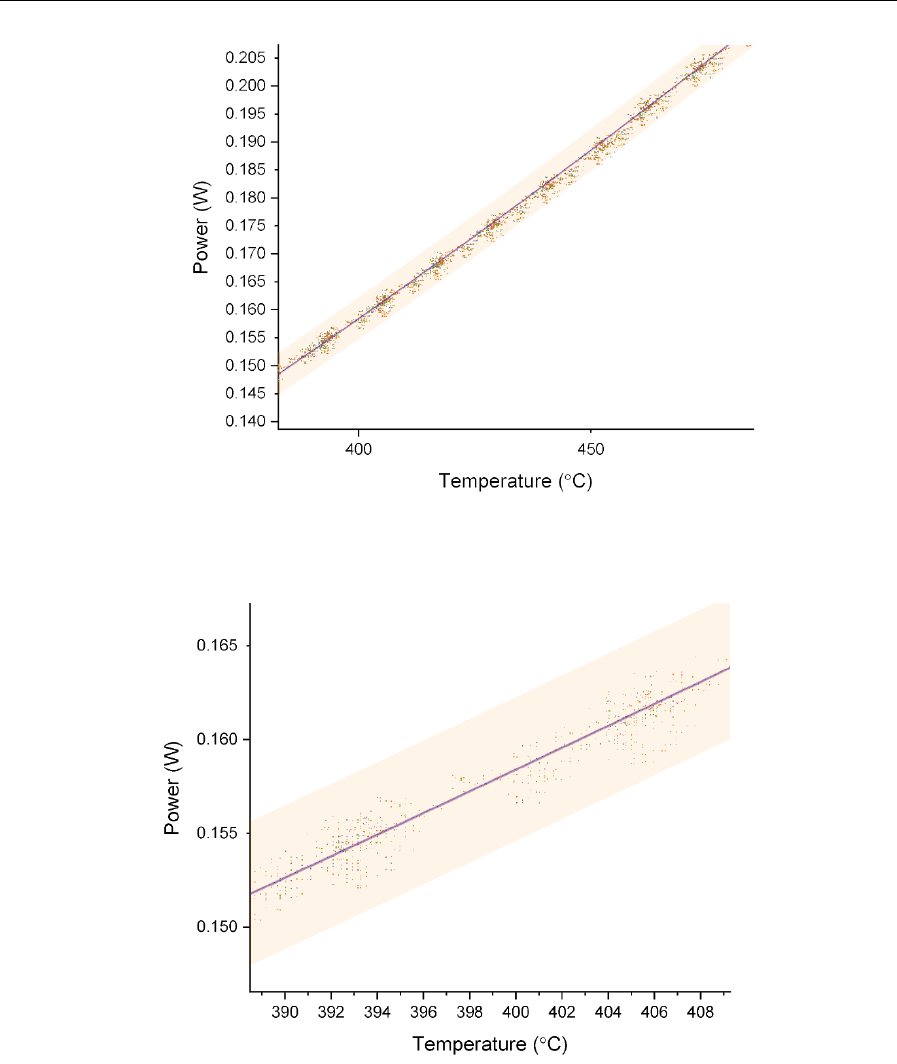
Figure 7 shows the same data as were used to plot Fig. 6, but plotted as power vs. temperature, with the
power calculated from the voltage drop across the active part of the sensor. Figure 8 through Fig. 10 are from
the same data set and show increasing levels of detail. All the sensors (with 100 nm platinum and those with
85 nm platinum, as mentioned previously) follow the same power-temperature relationship, providing an
alternative method to deduce the resistance-temperature curve, with slightly higher uncertainty than the
pyrometer method.

Volume 124, Article No. 124021 (2019) https://doi.org/10.6028/jres.124.021
Journal of Research of the National Institute of Standards and Technology
7 https://doi.org/10.6028/jres.124.021
Fig. 6. Elevated-temperature calibration data for 100 randomly selected sensors. This data set falls into two groups, as one production
batch had an inadvertently thinner layer of platinum, which resulted in approximately 15 % higher resistance than our normal process. One
should note that both the slope and intercept vary from sensor to sensor. The intention of this figure is to show the scatter in the data and
the importance of calibrating each nanocalorimeter individually. We have not tried to fit all these data points to a single line or curve
because the error would be dramatic.
Fig. 7. Power as a function of temperature for the same 100 randomly selected sensors (approximately 6300 data points) shown in Fig. 6.
The processing differences, seen as two separate groups on the resistance-temperature graphs, are not apparent in these power-temperature
curves. The fit was constrained to room temperature at zero power. The orange band is the 95 % confidence prediction interval. The colors
represent each of the 100 randomly selected nanocalorimeter data sets, but the data fall very close together and cannot be distinguished,
even with fine markers and lines.
Volume 124, Article No. 124021 (2019) https://doi.org/10.6028/jres.124.021
Journal of Research of the National Institute of Standards and Technology
8 https://doi.org/10.6028/jres.124.021
Fig. 8. More detailed view of the data in Fig. 7. The orange band is the 95 % confidence prediction interval. The colors represent each of
the 100 randomly selected nanocalorimeter data sets, but the data fall very close together and cannot be distinguished, even with fine
markers and lines.
Fig. 9. More detailed view of the data in Fig. 8. The orange band is the 95 % confidence prediction interval. The colors represent each of
the 100 randomly selected nanocalorimeter data sets.
Knowing the power-temperature relationship, which would vary with the type of nanocalorimeter used,
and the gas environment, allows one to heat each empty sensor, record the voltage and current, calculate the
power and resistance, and then deduce the sensor temperature from the power data to generate a temperature-
resistance calibration curve for each sensor.
In addition, Fig. 7 through Fig. 10 show that all 100 of the sensors we included fell along a well-defined
curve.

Volume 124, Article No. 124021 (2019) https://doi.org/10.6028/jres.124.021
Journal of Research of the National Institute of Standards and Technology
9 https://doi.org/10.6028/jres.124.021
Fig. 10. More detailed view of the data in Fig. 9. The orange band (which fills the field of view) is the 95 % confidence prediction interval.
The 95 % confidence interval of the fit is shown in the purple band; it is indistinguishable from the fit line in the other views. The colors
represent each of the 100 randomly selected nanocalorimeter data sets, but the data fall very close together and cannot be distinguished,
even with fine markers and lines.
This relationship can also be used as a type of “built-in self-test” (BIST) [38, 40] to verify the device was
fabricated and calibrated correctly. Any points or sensors that do not fall on this line should be considered
suspect and should be retested or investigated to understand the anomaly. The polynomial fit shown in Fig. 5
has an R
2
value of 0.99993, with units of watts and degrees Celsius:
Power = −5.68 × 10
−3
+ 2.3966 × 10
−4
× T + 4.2645 × 10
−7
× T
2
. (1)
Confidence intervals were calculated using Origin software. The definitions of the confidence intervals
reported below are available at https://www.originlab.com/doc/Origin-Help/Fitted_Curve_Plot_Analysis. The
95 % confidence interval for the fit reports the range of values for the best-fit line that define the 95 %
confidence interval. The 95 % confidence interval for the prediction is the range where 95 % of experimental
data points are expected to fall. The 95 % confidence interval of the fit is indistinguishable from the fit line in
most views of this data set and is shown in a purple band that can be resolved only in Fig. 10. At 190 mW, the
95 % confidence interval of the fit is 452.30 °C to 452.43 °C (or ± 0.065 °C).
The 95 % confidence interval for the prediction is shown in the orange band and varies with power level.
At 50 mW, the 95 % confidence prediction interval is 167 °C to 186 °C (or ± 9.5 °C). At 150 mW, the 95 %
confidence prediction interval is 379 °C to 392 °C (or ± 6.5 °C). At 250 mW, the 95 % confidence prediction
interval is 537 °C to 548 °C (or ± 5.5 °C). At 350 mW, the 95 % confidence prediction interval is 670 °C to
679 °C (or ± 4.5 °C).
7. Calibration
7.1 Virtual Instrument
Calibration is performed on a special-built instrument, with an automated process run through a LabVIEW
virtual instrument (VI). The VI was written at NIST for the Nanocalorimetry Measurements Project. Upon
starting the VI, the user creates or edits a calibration recipe, as shown in Fig. 11. A typical recipe, with three
cycles to measure the room-temperature resistance, three heating cycles, and three more cycles to confirm the
room-temperature resistance, is shown. As can be seen in Fig. 12, the user enters the type of measurement, the

Volume 124, Article No. 124021 (2019) https://doi.org/10.6028/jres.124.021
Journal of Research of the National Institute of Standards and Technology
10 https://doi.org/10.6028/jres.124.021
number of repetitions, the minimum voltage, the maximum voltage, the voltage step, and the number of
measurements per step. The VI calculates the estimated duration based on the entered information. Figure 13
shows the VI after running an experiment.
Each sensor is given a unique identifier (ID), which is entered along with the operator ID. The fiber-optic
pyrometer is aligned for each measurement, following the steps outlined below. The VI applies the voltage to
the sensor and measures the current in the measurement loop and the voltage across the voltage pads on the
sensor. A second VI, shown in Fig. 14, is used to calculate the TCR, which is saved into a data file to be used
by the VI that controls the nanocalorimeter experiments. A paper log is also maintained as a redundant record
with the sample ID and calibration coefficients. The detailed steps of the calibration procedure are included in
the supplemental information available online.
Fig. 11. A screen capture of the “Edit Recipe” window showing an example recipe used to calibrate the nanocalorimeter sensors. This
recipe produces three “before” room-temperature measurements, three up-and-down temperature ramps, and three “after” room-
temperature measurements.
Fig. 12. Screen capture of the main VI for nanocalorimeter sensor calibration, before starting a calibration. The recipe is shown in the
upper left, and the data will populate the other windows as they are collected. The software predicts the calibration measurements and
heating/cooling cycles for this recipe will take 14 min and 20 s.

Volume 124, Article No. 124021 (2019) https://doi.org/10.6028/jres.124.021
Journal of Research of the National Institute of Standards and Technology
11 https://doi.org/10.6028/jres.124.021
Fig. 13. Screen capture of the main VI for nanocalorimeter sensor calibration, after running the measurements for a calibration.
Fig. 14. Screen capture of the VI used to calculate the TCR values, based on the calibration recipe and data acquired as shown in Fig. 13.
This VI imports the six room-temperature resistance scans and the three heating and cooling scans and fits them to a fourth-order
polynomial used for the TCR. Other fits can be selected as well.
7.2 Calibration Extrapolation
This calibration strategy is valid for measurements within the range of the temperature measurements
made (approximately room temperature to 700 °C). We have successfully made measurements using these
sensors to 1200 °C, but that requires either increasing the calibration range or extrapolating the calibration
values to temperatures outside the range of measurement, something that will rapidly expand the measurement
uncertainty. As an example, Figs. 15 and 16 illustrate efforts to extrapolate the calibration outside the
measurement range. In Fig. 15, each fit is plotted with and without inclusion of the room-temperature
resistance value as a constraint. Some of the fits fail dramatically.

Volume 124, Article No. 124021 (2019) https://doi.org/10.6028/jres.124.021
Journal of Research of the National Institute of Standards and Technology
12 https://doi.org/10.6028/jres.124.021
The experimentally determined melting point for gold is shown in Fig. 16, along with two fits that worked
better and do not “blow up” outside the measurement range. Figure 16 shows a linear fit and a second-order
polynomial fit, both including the room-temperature constraint. They are off by 96 °C and 62 °C, respectively,
evaluated at the resistance recorded at the top of the melting peak (32.87 Ω, corresponding to a nominal
temperature of 1064.18 °C), which was measured in air.
Figure 17 shows the extrapolation of the power-temperature curve to the melting point of the same gold
thin film sample. The difference between the nominal peak melting temperature and the temperature derived
from the curve fit is 10 °C, which is much better than the error due to extrapolating the resistance-temperature
curve. These values are enumerated to illustrate the comparison and are not meant to quantify the uncertainty.
Fig. 15. Various fits through the calibration measurements (blue squares) that could potentially be used to extrapolate the calibration data
to higher temperatures. The graph shows linear, 2
nd
order polynomial, 4
th
order polynomial and a fit following the form of the Callendar-
Van Dusen (CVD) equation. The divergences seen with some fits outside the data range clearly illustrates the hazard in choosing a method
to extrapolate calibrations outside the measured range. For each, the fits were performed including the room-temperature (RT) data (pink,
dark green, light orange, light blue) or ignoring the room-temperature data (light green, purple, dark blue, dark orange).

Volume 124, Article No. 124021 (2019) https://doi.org/10.6028/jres.124.021
Journal of Research of the National Institute of Standards and Technology
13 https://doi.org/10.6028/jres.124.021
Fig. 16. Diagram showing the linear (blue line, R
2
= 0.9992) and second-order polynomial (orange line, R
2
= 0.9998) fits from Fig. 15,
extrapolated to higher temperatures, along with an experimentally measured (peak) value for the melting of gold (red dot, nominal 1064.18
°C and measured 32.87 Ω) as an example of a known melting peak at higher temperatures. The second-order polynomial fit extrapolates to
1002 °C at 32.87 Ω, and the linear fit extrapolates to 968 °C at 32.87 Ω; compared to the nominal melting temperature of the gold thin
film, the extrapolated fits are 62 °C to 96 °C too low. This example is given for information and is not intended as a quantification of
uncertainty. These fits included the room-temperature data.
Fig. 17. The same data and second-order polynomial from Fig. 7, extrapolated to higher temperatures, as another potential strategy to
extrapolate the calibration to higher temperatures. The orange line is the fit. An experimentally determined point (blue dot) for the melting
peak of a 65 nm layer of gold (nominal 1064.18 °C and measured 724.9 mW) is shown as an example of the error from extrapolating the
power-temperature curve—it is off by 10 °C at 1064 °C. This example is given for information and is not intended as a quantification of
uncertainty. As in Fig. 7 and Fig. 16, the curve fit was constrained to pass through zero power at room temperature.

Volume 124, Article No. 124021 (2019) https://doi.org/10.6028/jres.124.021
Journal of Research of the National Institute of Standards and Technology
14 https://doi.org/10.6028/jres.124.021
8. Discussion
This article summarizes the design and calibration of NIST nanocalorimeter sensors and presents
calibration data and analysis from 100 randomly selected sensor chips. Calibration using a pyrometer, with the
temperatures verified against melting point standards, remains our best calibration strategy.
Extrapolating resistance-temperature values to higher temperatures greatly increases the measurement
uncertainty. The power-temperature relationship can provide reasonable calibrations, without needing
expensive equipment, and offers uncertainties (95 % confidence interval for the prediction) that range from 5
°C to 10 °C, depending on the measurement temperature, and it provides a means to extrapolate the calibration
to higher temperatures without dramatically changing the measurement uncertainty.
9. Appendix—Detailed Fabrication and Calibration Procedures
The general strategy for the fabrication of the nanocalorimeters is to start with standard 100 mm (4 inch
nominal) wafers, clean them thoroughly, grow 100 nm of low-stress silicon nitride on the front and back,
pattern the platinum heater/temperature sensor on the front, use reactive ion etching to open windows in the
silicon nitride on the back, and then use potassium hydroxide (KOH) to deep etch from the back, through the
silicon wafer, stopping at the front-side silicon nitride layer, followed by dicing, annealing, and calibration.
9.1 Detailed Fabrication Process Developed for the CNST Cleanroom at NIST
9.1.1 This process requires two 5 inch (12.7 cm) chrome-on-glass masks—one for the front-side and
one for the back-side patterns. The masks were produced in AutoCAD and saved in data
exchange format (DXF). The masks were written using a Heidelberg DWL 2000 mask writer.
Links to the DXF files are listed in supplemental materials.
9.1.2 The silicon wafers are P/Bo doped, 1–10 ohm-cm, 100 mm (4 in. nominal) double-side polished,
<100> orientation, nominally 525 µm thick (the specification is given as a range of 500 µm to
550 µm).
9.1.3 All reagents used are microelectronics grade. All water used is deionized to cleanroom
specifications.
9.1.4 RCA clean
9.1.4.1 Standard Clean (SC) 1 (SC1) (5:1:1 H
2
O:NH
4
OH:H
2
O
2
at 80 °C) for 10 min
9.1.4.2 Dump rinse
9.1.4.3 1 % HF for 1 min
9.1.4.4 Dump rinse
9.1.4.5 SC2 (5:1:1 H
2
O:HCl:H
2
O
2
at 80 °C) for 10 min
9.1.4.6 Dump rinse
9.1.4.7 Spin rinse dry (SRD)
9.1.5 Silicon nitride deposition (front and back) SiN
x
9.1.5.1 Deposition is by Low Pressure Chemical Vapor Deposition (LPCVD) furnace/bank
3_silicon nitride
9.1.5.2 Low-stress recipe (LSTSIN.010)
9.1.5.3 Nominal 100 nm thickness
9.1.5.4 Calculate deposition time based on posted deposition rate (typical rate is 5.85 nm/min)
9.1.5.5 Measure and record thickness using J. A. Woollam M-2000 DI Spectroscopic Ellipsometer
9.1.6 Frontside metal patterning by lift-off process
9.1.6.1 Photolithography step
9.1.6.1.1. Hexamethyldisilazane (HMDS) prime (vapor prime at 150 °C)
9.1.6.1.2. Spin 1 (LOR-3A photoresist, target 400 nm thickness)
9.1.6.1.2.1. 500 rpm, 5.0 s
9.1.6.1.2.2. 3000 rpm, 60.0 s
9.1.6.1.2.3. Bake at 200 °C for 5 min
9.1.6.1.2.4. Cool for 5 min

Volume 124, Article No. 124021 (2019) https://doi.org/10.6028/jres.124.021
Journal of Research of the National Institute of Standards and Technology
15 https://doi.org/10.6028/jres.124.021
9.1.6.1.3. Spin 2 (S-1813 photoresist, target 1.3 µm)
9.1.6.1.3.1. 500 rpm, 5.0 s
9.1.6.1.3.2. 4000 rpm, 45.0 s
9.1.6.1.3.3. Bake at 115 °C for 1 min
9.1.6.1.3.4. Cool for 1 min
9.1.6.1.4. Expose (Suss MA6/BA6 mask aligner)
9.1.6.1.4.1. Frontside metal mask
9.1.6.1.4.2. Calculate and use exposure time based on lamp intensity (target dose 120 mJ/cm
2
)
9.1.6.1.5. Develop
9.1.6.1.5.1. MF-319, 1 min (or until features are clear)
9.1.6.1.5.2. Rinse with H
2
O
9.1.6.1.5.3. Blow dry
9.1.6.1.6. Oxygen plasma descum
9.1.6.1.6.1. Unaxis Reactive Ion Etch (RIE) #1
9.1.6.1.6.2. Recipe: G_DESCUM.PRC (target 75 nm/min), 1 min
9.1.7 Metal deposition step
9.1.7.1 E-beam evaporation (E-beam 1 or 2)
9.1.7.1.1. Nominal 10 nm Ta at 1 Å/s (typically 100 s)
9.1.7.1.2. Nominal 100 nm Pt at 1 Å /s (typically 1000 s)
9.1.8 Lift-off step
9.1.9 Remover PG at 80 °C for ≈ 15 min (Remover PG is a proprietary composition that includes
hexamethyldisilazane).
9.1.10 Rinse
9.1.10.1 Isopropyl alcohol (IPA) for 3 min
9.1.10.2 Water for 3 min
9.1.11 Spin rinse dry
9.1.12 Protect front side with photoresist (more experienced users may omit)
9.1.12.1 HMDS prime
9.1.12.2 Spin 1 (photoresist S-1813, nominal 1.3 µm)
9.1.12.3 500 rpm, 5.0 s
9.1.12.4 4000 rpm, 45.0 s
9.1.12.5 Bake at 115 °C for 1 min
9.1.12.6 Cool for 1 min
9.1.13 Backside nitride patterning
9.1.13.1 Photolithography step
9.1.13.1.1. HMDS prime
9.1.13.1.2. Spin 1 (photoresist S-1813, nominal 1.3 µm)
9.1.13.1.2.1. 500 rpm, 5.0 s
9.1.13.1.2.2. 4000 rpm, 45.0 s
9.1.13.1.2.3. Bake at 115 °C for 1 min
9.1.13.1.2.4. Cool for 1 min
9.1.13.1.3. Expose back side (Suss MA6/BA6 aligner)
9.1.13.1.3.1. Back-side nitride mask
9.1.13.1.3.2. Align with existing pattern
9.1.13.1.3.3. Calculate exposure time based on lamp intensity (target 120 mJ/cm
2
)
9.1.13.1.4. Develop
9.1.13.1.4.1. MF-319, 1 min (or until features are clear). (MF-319 is a proprietary
composition that includes water and tetramethylammonium hydroxide).
9.1.13.1.4.2. Rinse with deionized water
9.1.13.1.4.3. Blow dry
9.1.13.2 RIE CHF
3
etch (Unaxis RIE #1)
9.1.13.2.1. Recipe “SI3N4NEW.PRC,” nominal etch rate 20 nm/min

Volume 124, Article No. 124021 (2019) https://doi.org/10.6028/jres.124.021
Journal of Research of the National Institute of Standards and Technology
16 https://doi.org/10.6028/jres.124.021
9.1.13.2.2. Calculate etch time based on expected nitride thickness with 10 %
overetch time
9.1.13.2.3. Typical etch time is: 100 nm ÷ 20 nm/min × 1.1 = 5.5 min
9.1.13.3 Oxygen plasma cleaning (to remove rest of photoresist, may require both sides)
9.1.13.4 Unaxis RIE #1
9.1.13.5 Recipe: Cleaning.PRC
9.1.13.6 15 min
9.1.13.7 (Note: Solvent strip with remover PG is an acceptable alternative)
9.1.14 Back-side deep silicon KOH etch
(Note: The wafer is very fragile during and after this step)
(Note: Always insert wafer into liquids on edge)
9.1.14.1 30 % KOH (premixed bath), 90 °C
9.1.14.1.1. (Note: Do not use old KOH baths to avoid metal contamination and photoresist
residue left over from other users)
9.1.14.2 Clamp wafer in protective holder (Advanced MicroMachining Tools, Single 4) and place in
protective wafer carrier—do not use photoresist as a KOH etch mask because it is not sufficient
AND will contaminate the bath
9.1.14.3 No agitation
9.1.14.4 Nominal rate is 2.25 µm/min for 30 % KOH at 90 °C
9.1.14.5 Nominal etch time: 230 min (it will not be this exactly—check, and continue until features
are clear)
9.1.14.6 Avoid over etching
9.1.14.7 Acid dip (note: Do not let KOH residue dry)
9.1.14.8 Rinse with wafer still in holder:
9.1.14.8.1. Warm water for 1 min
9.1.14.8.2. Over flow water for 5 min
9.1.14.8.3. Water dunk (membranes up)
9.1.14.8.4. Gentle dry with wipe around edge of holder
9.1.14.9 Remove wafer from holder
9.1.15 Cleave by hand into individual die with a diamond scribe (note: other users have reported
using photoresist to attach the wafer to a handle wafer and using a die saw to separate the die; the
membranes will not survive the vacuum chuck on the die saw without some approach like this; we
choose just to cleave by hand)
9.1.16 Anneal
9.2 Calibration Procedure
9.2.1 Turn on the instruments and let them warm up for at least half an hour to stabilize if they
were turned off
9.2.1.1 OPTITHERM III Pyrometer
9.2.1.2 National Instruments PXI Chassis and PXI Sourcemeter PXI-1033
9.2.1.3 Dell personal computer (PC)
9.2.1.4 Water circulator (if being used to stabilize room temperature)
9.2.2 Load two nanocalorimeter sensors in the aluminum holder and secure the top of the holder
with four screws; the electrical connections are made with spring pins in the top of the holder
9.2.3 On the PC, open the LabVIEW calibration VI “Calibrate Nanocalorimeter Chip.vi”
9.2.3.1 Enter user ID
9.2.4 Confirm settings within the VI
9.2.4.1 Source Measure Unit (SMU) location = PXI1Slot2 (this would vary by instrument)
9.2.4.2 Sensor type = remote
9.2.4.3 Pyrometer port = COM7

Volume 124, Article No. 124021 (2019) https://doi.org/10.6028/jres.124.021
Journal of Research of the National Institute of Standards and Technology
17 https://doi.org/10.6028/jres.124.021
9.2.4.4 Current limit = 300 mA
9.2.4.5 Ambient temperature = 23 °C
9.2.5 Create or load a saved recipe (an example is given in Fig. 6)
9.2.6 Turn the screw on the manual stage to move the pyrometer head forward and above the
sensor to be calibrated
9.2.7 Align the pyrometer
9.2.7.1 Enable SMU
9.2.7.2 Enable pyrometer
9.2.7.3 Increase voltage to 1.8 V (a typical value), so the sensor heats enough to generate a signal on
the pyrometer
9.2.7.4 Move the pyrometer head in forward and backward to find the maximum reported
temperature value (which is taken to be the center)
9.2.7.5 Set the voltage range for the calibration
9.2.7.5.1. In the VI, decrease the applied voltage to find the minimum voltage where the
pyrometer can make a measurement (about 1.45 V, which corresponds to a temperature of
about 320 °C on this sensor)
9.2.7.5.2. Disable SMU and pyrometer
9.2.7.5.3. Set the minimum voltage for a sweep to the minimum plus 0.01 V (1.50 V is
common)
9.2.7.5.4. Set the maximum voltage based on the temperature range over which you wish to
calibrate (3.1 volts at the SMU is common, with roughly 1.5 volts differential across the
sensor and a maximum temperature of 675 °C)
9.2.8 Calibration
9.2.8.1 Start calibration by clicking on the “start calibration” button
9.2.8.2 Enter a calibration file name and location
9.2.8.3 Enter the results in the paper log as a redundant record
9.2.8.4 When completed, calibrate the second sensor if desired
9.2.8.4.1. Shift the pyrometer to the second sensor location
9.2.8.4.2. Turn the sensor switch to the other sensor
9.2.8.4.3. Enter the new sensor ID
9.2.8.4.4. Repeat the procedure from the alignment step (see Sec. 8.2.7)
9.2.8.4.5. Move the pyrometer head out of the way and unload the samples, storing them in
numbered locations
9.2.9 Click the “exit” button to close the VI
9.2.10 Calculate the TCR values
9.2.10.1 Open the VI “TCR analysis-mod-071511.vi”
9.2.10.2 Select each of the data files to use in the analysis and click “cancel” to return to the VI
9.2.10.3 Run the VI to calculate the TCR values
9.2.10.4 Examine the fit and reported uncertainties as a quality check
9.2.10.5 Save the results as a “.tcr” file format
9.2.10.6 Record the TCR values in the paper log
9.2.10.7 Exit
Supplemental Materials
• DOI: https://doi.org/10.18434/M32113
o AutoCAD drawing files for the front and back 5 inch (12.7 cm) masks needed to pattern 100 mm
(4 inch [10.1 cm]) wafers. Files are in both AutoCAD DWG format and DXF format. The
drawing for the back-side mask has been mirrored as is appropriate for lithography using a
contact aligner.
• DOI: https://doi.org/10.18434/M32114
o 3D solid model of a single nanocalorimeter as a Solidworks assembly drawing, with individual
layers as Solidworks part drawings.

Volume 124, Article No. 124021 (2019) https://doi.org/10.6028/jres.124.021
Journal of Research of the National Institute of Standards and Technology
18 https://doi.org/10.6028/jres.124.021
• DOI: https://doi.org/10.18434/M32117
o Compressed archive of LabVIEW VIs for calibration and TCR calculation.
• DOI: https://doi.org/10.18434/M32115
o Calibration data for room-temperature measurements shown in Fig. 2 through Fig 5.
o Calibration data for elevated-temperature measurements on 100 randomly selected
nanocalorimeters shown in Fig. 6 through Fig. 10.
10. References
[1] Arlington SQ, Yi F, LaVan DA, Weihs TP (2019) A nanocalorimetric study of the effect of composition gradients on crystallization
in amorphous Cu-Zr thin films. AIP Advances 9(3). https://doi.org/10.1063/1.5080312
[2] DeLisio JB, Yi F, LaVan DA, Zachariah MR (2017) High heating rate reaction dynamics of Al/CuO nanolaminates by
nanocalorimetry-coupled time-of-flight mass spectrometry. Journal of Physical Chemistry C 121(5):2771-2777.
https://doi.org/10.1021/acs.jpcc.6b11114
[3] Franke E, LaVan DA, Volkert CA (2018) Quantifying DC differential scanning nanocalorimetry for determining heat capacities.
Thermochimica Acta 668:116-125. https://doi.org/10.1016/j.tca.2018.08.006
[4] Grapes MD, LaGrange T, Friedman LH, Reed BW, Campbell GH, Weihs TP, LaVan DA (2014) Combining nanocalorimetry and
dynamic transmission electron microscopy for in situ characterization of materials processes under rapid heating and cooling. Review
of Scientific Instruments 85(8): 084902-084901 to 084902-084912. https://doi.org/10.1063/1.4892537
[5] Grapes MD, LaGrange T, Woll K, Reed BW, Campbell GH, LaVan DA, Weihs TP (2014) In situ transmission electron microscopy
investigation of the interfacial reaction between Ni and Al during rapid heating in a nanocalorimeter. APL Materials 2(11).
https://doi.org/10.1063/1.4900818
[6] Grapes MD, Santala MK, Campbell GH, LaVan DA, Weihs TP (2017) A detailed study of the Al3Ni formation reaction using
nanocalorimetry. Thermochimica Acta 658:72-83. https://doi.org/10.1016/j.tca.2017.10.018
[7] Kummamuru RK, De La Rama L, Hu L, Vaudin MD, Efremov MY, Green ML, LaVan DA, Allen LH (2009) Measurement of heat
capacity and enthalpy of formation of nickel silicide using nanocalorimetry. Applied Physics Letters 95(18).
https://doi.org/10.1063/1.3255009
[8] Swaminathan P, Burke BG, Holness AE, Wilthan B, Hanssen L, Weihs TP, LaVan DA (2011) Optical calibration for
nanocalorimeter measurements. Thermochimica Acta 522(1-2):60-65. https://doi.org/10.1016/j.tca.2011.03.006
[9] Swaminathan P, Grapes MD, Woll K, Barron SC, LaVan DA, Weihs TP (2013) Studying exothermic reactions in the Ni-Al system at
rapid heating rates using a nanocalorimeter. Journal of Applied Physics 113(14). https://doi.org/10.1063/1.4799628
[10] Swaminathan P, LaVan DA, Weihs TP (2011) Dynamics of solidification in Al thin films measured using a nanocalorimeter. Journal
of Applied Physics 110(11). https://doi.org/10.1063/1.3668128
[11] Yi F, DeLisio JB, Nguyen N, Zachariah MR, LaVan DA (2017) High heating rate decomposition dynamics of copper oxide by
nanocalorimetry-coupled time-of-flight mass spectrometry. Chemical Physics Letters 689:26-29. https://doi.org/10.1016/j.cplett.2017.09.066
[12] Yi F, DeLisio JB, Zachariah MR, LaVan DA (2015) Nanocalorimetry-coupled time-of-flight mass spectrometry: identifying evolved
species during high-rate thermal measurements. Analytical Chemistry 87(19):9740-9744. https://doi.org/10.1021/acs.analchem.5b01872
[13] Yi F, Kim IK, Li S, LaVan DA (2014) Hydrated/dehydrated lipid phase transitions measured using nanocalorimetry. Journal of
Pharmaceutical Sciences 103(11):3442-3447. https://doi.org/10.1002/jps.24187
[14] Yi F , LaVan DA (2013) Electrospray-assisted nanocalorimetry measurements. Thermochimica Acta 569:1-7.
https://doi.org/10.1016/j.tca.2013.06.015
[15] Yi F, Osborn W, Betz J, LaVan DA (2015) Interactions of adhesion materials and annealing environment on resistance and stability
of MEMS platinum heaters and temperature sensors. Journal of Microelectromechanical Systems 24(4):1185-1192.
https://doi.org/10.1109/Jmems.2015.2394483
[16] Yi F, Stevanovic A, Osborn WA, Kolmakov A, LaVan DA (2017) A multi-environment nanocalorimeter with electrical contacts for
use in a scanning electron microscope. Materials Horizons 4(6):1128-1134. https://doi.org/10.1039/c7mh00513j
[17] de la Rama LP, Hu L, Ye ZC, Efremov MY, Allen LH (2013) Size effect and odd-even alternation in the melting of single and
stacked AgSCn layers: synthesis and nanocalorimetry measurements. Journal of the American Chemical Society 135(38):14286-
14298. https://doi.org/10.1021/ja4059958
[18] Efremov MY, Olson EA, Zhang M, Allen LH (2003) Glass transition of thin films of poly(2-vinyl pyridine) and poly(methyl
methacrylate): nanocalorimetry measurements. Thermochimica Acta 403(1):37-41. https://doi.org/10.1016/s0040-6031(03)00122-9
[19] Efremov MY, Olson EA, Zhang M, Lai SL, Schiettekatte F, Zhang ZS, Allen LH (2004) Thin-film differential scanning
nanocalorimetry: heat capacity analysis. Thermochimica Acta 412(1-2):13-23. https://doi.org/10.1016/j.tca.2003.08.019
[20] Efremov MY, Olson EA, Zhang M, Schiettekatte F, Zhang ZS, Allen LH (2004) Ultrasensitive, fast, thin-film differential scanning
calorimeter. Review of Scientific Instruments 75(1):179-191. https://doi.org/10.1063/1.1633000
[21] Efremov MY, Schiettekatte F, Zhang M, Olson EA, Kwan AT, Berry RS, Allen LH (2000) Discrete periodic melting point
observations for nanostructure ensembles. Physical Review Letters 85(17):3560-3563.
[22] Hu L, de la Rama LP, Efremov MY, Anahory Y, Schiettekatte F, Allen LH (2011) Synthesis and characterization of single-layer
silver-decanethiolate lamellar crystals. Journal of the American Chemical Society 133(12):4367-4376.
https://doi.org/10.1021/ja107817x

Volume 124, Article No. 124021 (2019) https://doi.org/10.6028/jres.124.021
Journal of Research of the National Institute of Standards and Technology
19 https://doi.org/10.6028/jres.124.021
[23] Lai SL, Carlsson JRA, Allen LH (1998) Melting point depression of Al clusters generated during the early stages of film growth:
Nanocalorimetry measurements. Applied Physics Letters 72(9):1098-1100. https://doi.org/10.1063/1.120946
[24] Olson EA, Efremov MY, Zhang M, Zhang Z, Allen LH (2005) Size-dependent melting of Bi nanoparticles. Journal of Applied
Physics 97(3). https://doi.org/10.1063/1.1832741
[25] Zhang M, Efremov MY, Olson EA, Zhang ZS, Allen LH (2002) Real-time heat capacity measurement during thin-film deposition by
scanning nanocalorimetry Applied Physics Letters 81(20):3801-3803. https://doi.org/10.1063/1.1520714
[26] Zhang M, Olson EA, Twesten RD, Wen JG, Allen LH, Robertson IM, Petrov I (2005) In situ transmission electron microscopy
studies enabled by microelectromechanical system technology. Journal of Materials Research 20(7):1802-1807.
https://doi.org/10.1557/jmr.2005.0225
[27] Zhang ZS, Wilson OM, Efremov MY, Olson EA, Braun PV, Senaratne W, Ober CK, Zhang M, Allen LH (2004) Heat capacity
measurements of two-dimensional self-assembled hexadecanethiol monolayers on polycrystalline gold. Applied Physics Letters
84(25):5198-5200. https://doi.org/10.1063/1.1764938
[28] Yi F, LaVan D (2019) Nanocalorimetry: Exploring materials faster and smaller. Applied Physics Reviews 6(3).
https://doi.org/https://doi.org/10.1063/1.5098297
[29] Davaji B, Bak HJ, Chang WJ, Lee CH (2014) A novel on-chip three-dimensional micromachined calorimeter with fully enclosed and
suspended thin-film chamber for thermal characterization of liquid samples. Biomicrofluidics 8(3). https://doi.org/10.1063/1.4875656
[30] Guenther G, Aulbach E, Hahn H, Guillon O (2011) High-temperature chip calorimeter with atmosphere control. Thermochimica Acta
522(1-2):77-85. https://doi.org/10.1016/j.tca.2011.03.013
[31] Johannessen EA, Weaver JMR, Cobbold PH, Cooper JM (2002) Heat conduction nanocalorimeter for pl-scale single cell
measurements. Applied Physics Letters 80(11):2029-2031. https://doi.org/10.1063/1.1457532
[32] Johannessen EA, Weaver JMR, Cobbold PH, Cooper JM (2002) A suspended membrane nanocalorimeter for ultralow volume
bioanalysis. IEEE Transactions on NanoBioscience 1(1):29-36. https://doi.org/10.1109/Tnb.2002.806935
[33] Minakov AA, Adamovsky SA, Schick C (2005) Non-adiabatic thin-film (chip) nanocalorimetry. Thermochimica Acta 432(2):177-
185. https://doi.org/10.1016/j.tca.2005.01.073
[34] Minakov AA, Roy SB, Bugoslavsky YV, Cohen LF (2005) Thin-film alternating current nanocalorimeter for low temperatures and
high magnetic fields. Review of Scientific Instruments 76(4). https://doi.org/10.1063/1.1889432
[35] Queen DR , Hellman F (2009) Thin film nanocalorimeter for heat capacity measurements of 30 nm films. Review of Scientific
Instruments 80(6).
https://doi.org/10.1063/1.3142463
[36] Suurkuusk J, Suurkuusk M, Vikegard P (2018) A multichannel microcalorimetric system the third-generation Thermal Activity
Monitor (TAM III). Journal of Thermal Analysis and Calorimetry 131(2):1949-1966. https://doi.org/10.1007/s10973-017-6684-7
[37] Xu J, Reiserer R, Tellinghuisen J, Wikswo JP, Baudenbacher FJ (2008) A microfabricated nanocalorimeter: design, characterization,
and chemical calibration. Analytical Chemistry 80(8):2728-2733. https://doi.org/10.1021/ac702213d
[38] Afridi M, Montgomery C, Cooper-Balis E, Semancik S, Kreider KG, Geist J (2011) Micro hotplate Temperature Sensor Calibration
and BIST. Journal of Research of the National Institute of Standards and Technology 116(6):827-838.
https://doi.org/10.6028/jres.116.025
[39] Afridi M, Montgomery CB, Cooper-Balis E, Semancik S, Kreider KG, Geist J (2009) Analog BIST functionality for microhotplate
temperature sensors. IEEE Electron Device Letters 30(9):928-930. https://doi.org/10.1109/Led.2009.2027038
[40] Afridi MY , Geist J (2010) MEMS Microhotplate temperature sensor BIST: importance and applications. IEEE Sensor:2159-2160.
https://doi.org/10.1109/Icsens.2010.5690549
[41] Dable BK, Booksh KS, Cavicchi R, Semancik S (2004) Calibration of microhotplate conductometric gas sensors by non-linear
multivariate regression methods. Sensors and Actuators B: Chemical 101(3):284-294. https://doi.org/10.1016/j.snb.2004.03.003
[42] Elmi I, Zampolli S, Dori L, Cardinali GC, Nicoletti S, Giovanelli G, Severi M (2005) A low cost transportable instrument based on
microsystem technologies for benzene monitoring in outdoor air: a comparative in-field test using a standard GC tool. WIT
Transactions on Ecology and the Environment 82:425-434.
[43] Thiery L, Toullier S, Teyssieux D, Briand D (2008) Thermal contact calibration between a thermocouple probe and a microhotplate.
Journal of Heat Transfer 130(9). https://doi.org/10.1115/1.2943306
[44] Wheeler MC, Tiffany JE, Walton RM, Cavicchi RE, Semancik S (2001) Chemical crosstalk between heated gas microsensor
elements operating in close proximity. Sensors and Actuators B: Chemical 77(1-2):167-176. https://doi.org/10.1016/S0925-
4005(01)00689-X
[45] Yi F, Friedman LH, Chen R, LaVan DA (2019) Sample pattern and temperature distribution in nanocalorimetry measurements.
Journal of Thermal Analysis and Calorimetry. https://doi.org/10.1007/s10973-019-08139-2
About the authors: Feng Yi is a research chemist in the Materials Measurement Science Division in the
Material Measurement Laboratory at NIST, working in nanocalorimetry. Michael D. Grapes was a graduate
student at Johns Hopkins University during this work, collaborating with NIST, and is currently a materials
scientist in the Materials Science Division, Physical and Life Sciences Directorate, at the Lawrence Livermore
National Laboratory. David A. LaVan is a materials scientist, mechanical engineer, and project leader in the
Materials Measurement Science Division in the Material Measurement Laboratory at NIST. His work focuses
on nanocalorimetry, MicroElectroMechanical Systems (MEMS), and sensors. The National Institute of
Standards and Technology is an agency of the U.S. Department of Commerce.
