
2009-2013 Microchip Technology Inc. DS70000582E-page 1
HIGHLIGHTS
This section of the manual contains the following major topics:
1.0 Introduction ....................................................................................................................... 2
2.0 Control Registers .............................................................................................................. 4
3.0 UART Baud Rate Generator ........................................................................................... 12
4.0 UART Configuration........................................................................................................ 14
5.0 UART Transmitter ........................................................................................................... 15
6.0 Data Bit Detection ...........................................................................................................20
7.0 UART Receiver ............................................................................................................... 21
8.0 Using the UART for 9-Bit Communication ...................................................................... 26
9.0 Other Features of the UART ........................................................................................... 29
10.0 UART Operation with DMA ............................................................................................. 31
11.0 UART Operation During CPU Sleep and Idle Modes ..................................................... 33
12.0 Operation of UxCTS and UxRTS Control Pins ............................................................... 35
13.0 Infrared Support .............................................................................................................. 37
14.0 LIN/J2602 Support.......................................................................................................... 40
15.0 Smart Card Support........................................................................................................ 42
16.0 Registers Map................................................................................................................. 51
17.0 Related Application Notes............................................................................................... 52
18.0 Revision History .............................................................................................................. 53
Universal Asynchronous Receiver Transmitter (UART)

dsPIC33/PIC24 Family Reference Manual
DS70000582E-page 2 2009-2013 Microchip Technology Inc.
This document supersedes the following PIC24 and dsPIC Family Reference Manual sections:
1.0 INTRODUCTION
The Universal Asynchronous Receiver Transmitter (UART) module is one of the serial I/O
modules available in the dsPIC33 and PIC24 device families. The UART is a full-duplex,
asynchronous communication channel that communicates with peripheral devices and personal
computers, using protocols such as RS-232, RS-485, LIN/J2602 and IrDA
®
. The module also
supports the hardware flow control option with the UxCTS
and UxRTS pins and includes the IrDA
encoder and decoder.
The primary features of the UART module are as follows:
• Full-duplex, 8-bit or 9-bit data transmission through the UxTX and UxRX pins
• Even, odd or no parity options (for 8-bit data)
• One or two Stop bits
• Hardware auto-baud feature
• Hardware flow control option with the UxCTS
and UxRTS pins (These pins are not
available on all devices. Refer to the “Universal Asynchronous Receiver Transmitter
(UART)” chapter of the specific device data sheet for availability.)
• Fully integrated Baud Rate Generator (BRG) with 16-bit prescaler
• Baud rates up to 17.5 Mbps
• Four-deep First-In First-Out (FIFO) transmit data buffer
• Four-deep FIFO receive data buffer
• Parity, framing and buffer overrun error detection
• Support for 9-bit mode with address detect (9th bit = 1)
• Transmit and receive interrupts
• Loopback mode for diagnostic support
• IrDA encoder and decoder logic
• LIN/J2602 bus support (v1.3 and 2.0)
• 16x baud clock output for external IrDA encoder/decoder support
• Optional ISO 7816 Smart Card support
Note: This family reference manual section is meant to serve as a complement to device
data sheets. Depending on the device variant, this manual section may not apply to
all dsPIC33 and PIC24 devices.
Please consult the note at the beginning of the “Universal Asynchronous
Receiver Transmitter (UART)” chapter in the current device data sheet to check
whether this document supports the device you are using.
Device data sheets and family reference manual sections are available for download
from the Microchip worldwide web site at: http://www.microchip.com
DS Number Section Number Title
DS39708 21 UART: PIC24F Family Reference Manual
DS70232 17 UART: PIC24H Family Reference Manual
DS70582 17 UART: dsPIC33E/PIC24E Family Reference Manual
DS70066 19, 34 UART: dsPIC30F Family Reference Manual
DS70188 17 UART: dsPIC33F/PIC24H Family Reference Manual
DS70582 17 UART: dsPIC33E/PIC24E Family Reference Manual

2009-2013 Microchip Technology Inc. DS70000582E-page 3
UART
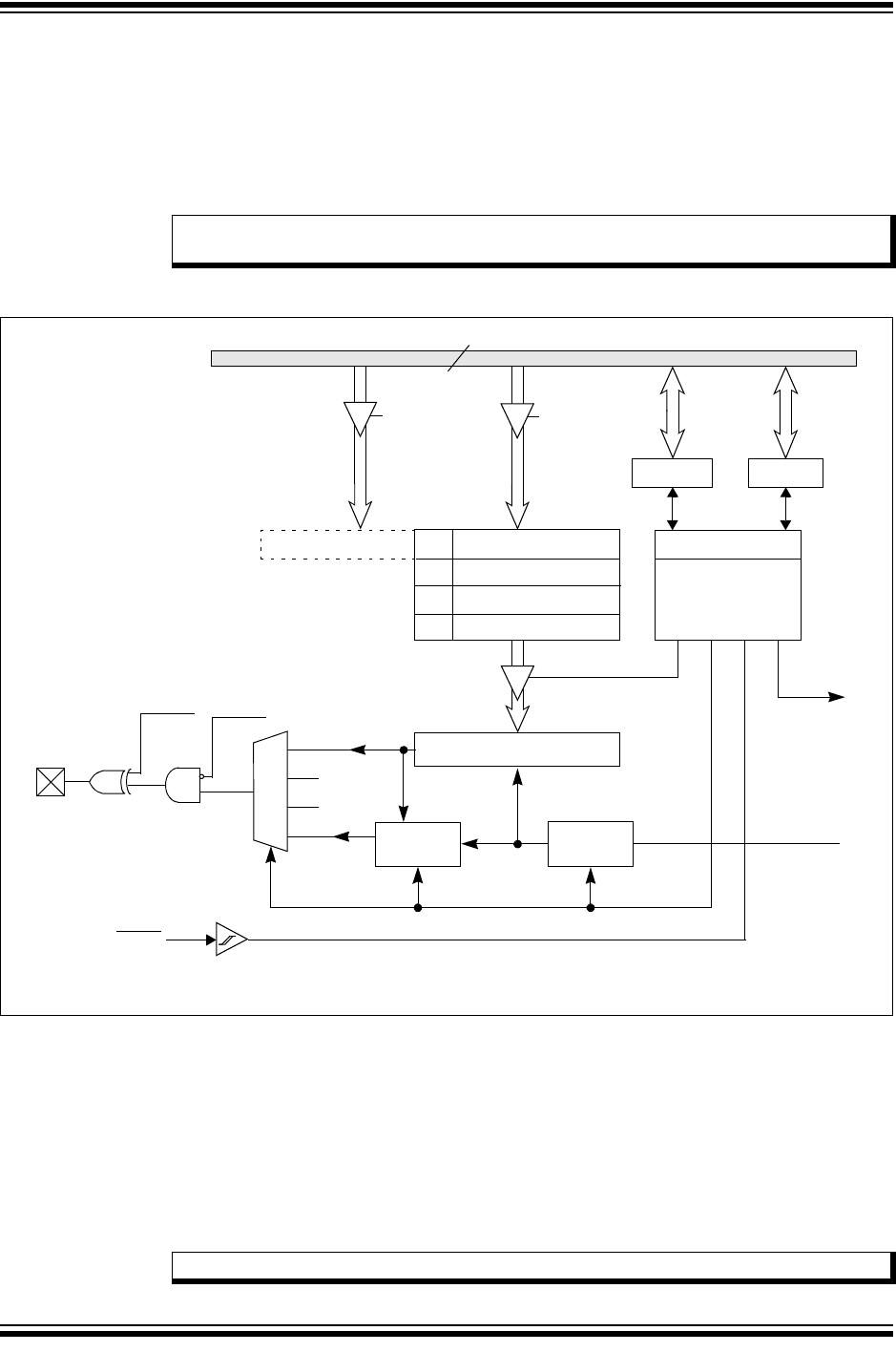
A simplified block diagram of the UART is illustrated in Figure 1-1. The UART module consists
of the following key hardware elements:
• Baud Rate Generator
• Asynchronous Transmitter
• Asynchronous Receiver
Figure 1-1: UARTx Simplified Block Diagram
Baud Rate Generator
UxRX
Hardware Flow Control
UARTx Receiver
UARTx Transmitter
UxTX
UxCTS
UxRTS
BCLKx
ISO 7816 Support
IrDA
®

dsPIC33/PIC24 Family Reference Manual
DS70000582E-page 4 2009-2013 Microchip Technology Inc.
2.0 CONTROL REGISTERS
This section outlines the specific functions of each register that controls the operation of the
UART module:
• UxMODE: UARTx Mode Register
- Enables or disables the UART module
- Enables or disables the IrDA encoder and decoder
- Enables or disables the WAKE, ABAUD bits and Loopback features
- Enables or disables the UxRTS
and UxCTS pins
- Configures the UxRTS pin for the desired mode of operation
- Configures the polarity of the UxRX pin
- Selects the type of baud rate
- Selects the number of data bits, parity and Stop bits
• UxSTA: UARTx Status and Control Register
- Selects the Transmission Interrupt mode
- Selects the Receive Interrupt mode
- Enables or disables the UART transmission
- Controls the Address Detect mode
- Indicates various status conditions, such as transmit and receive buffer state, parity
error, framing error and overflow error
• UxADMD: UARTx Address Mask Detect Register
- Stores address match and mask values
• UxRXREG: UARTx Receive Register
- Stores the received data
• UxTXREG: UARTx Transmit Register (Write-Only)
- Provides the data to be transmitted
• UxBRG: UARTx Baud Rate Register
- Stores the baud rate value of the transmitted or received data
Note: Each dsPIC33/PIC24 family device variant may have one or more UART modules.
An ‘x’ used in the names of pins, control/status bits and registers denotes the par-
ticular UART module number. Refer to the “Universal Asynchronous Receiver
Transmitter (UART)” chapter of the specific device data sheet for more details.

2009-2013 Microchip Technology Inc. DS70000582E-page 5
UART
Register 2-1: UxMODE: UARTx Mode Register
R/W-0 U-0 R/W-0 R/W-0 R/W-0 R/W-0 R/W-0 R/W-0
UARTEN
(3)
— USIDL IREN
(1)
RTSMD ALTIO
(2)
UEN1
(2)
UEN0
(2)
bit 15 bit 8
R/W-0 R/W-0 R/W-0 R/W-0 R/W-0 R/W-0 R/W-0 R/W-0
WAKE
(4)
LPBACK ABAUD
(5)
URXINV BRGH PDSEL1 PDSEL0 STSEL
bit 7 bit 0
Legend:
R = Readable bit W = Writable bit U = Unimplemented bit, read as ‘0’
-n = Value at POR ‘1’ = Bit is set ‘0’ = Bit is cleared x = Bit is unknown
bit 15 UARTEN: UARTx Enable bit
(3)
1 = UARTx is enabled; UARTx pins are controlled by UARTx as defined by the UEN<1:0> and
UTXEN control bits
0 = UARTx is disabled; UARTx pins are controlled by the corresponding PORTx, LATx and TRISx bits
bit 14 Unimplemented: Read as ‘0’
bit 13 USIDL: UARTx Stop in Idle Mode bit
1 = Discontinues operation when the device enters Idle mode
0 = Continues operation in Idle mode
bit 12 IREN: IrDA
®
Encoder and Decoder Enable bit
(1)
1 = IrDA encoder and decoder are enabled
0 = IrDA encoder and decoder are disabled
bit 11 RTSMD: Mode Selection for UxRTS
Pin bit
1 = UxRTS is in Simplex mode
0 = UxRTS
is in Flow Control mode
bit 10 ALTIO: UARTx Alternate I/O Selection bit
(2)
1 = UARTx communicates using UxATX and UxARX I/O pins
0 = UARTx communicates using UxTX and UxRX I/O pins
bit 9-8 UEN<1:0>: UARTx Enable bits
(2)
11 = UxTX, UxRX and BCLKx pins are enabled and used; UxCTS pin is controlled by port latches
10 = UxTX, UxRX, UxCTS
and UxRTS pins are enabled and used
01 = UxTX, UxRX and UxRTS
pins are enabled and used; UxCTS pin is controlled by port latches
00 = UxTX and UxRX pins are enabled and used; UxCTS
, UxRTS and BCLKx pins are controlled by
port latches
bit 7 WAKE: Enable Wake-up on Start bit Detect During Sleep Mode bit
(4)
1 = Wake-up is enabled
0 = Wake-up is disabled
bit 6 LPBACK: UARTx Loopback Mode Select bit
1 = Enables Loopback mode
0 = Loopback mode is disabled
Note 1: This feature is only available for Standard Speed mode (BRGH = 0). Refer to the “Universal Asynchronous
Receiver Transmitter (UART)” chapter of the specific device data sheet for availability.
2: These features may not be available on all devices. Refer to the “Universal Asynchronous Receiver
Transmitter (UART)” chapter of the specific device data sheet for availability.
3: Enable this bit before enabling the UTXEN bit (UxSTA<10>).
4: The UARTx module does not recognize the first character received on a wake.
5: The use of this feature may consume the corresponding Input Capture x (ICx) peripheral. See Section 9.2
“Auto-Baud Support” for more information.

dsPIC33/PIC24 Family Reference Manual
DS70000582E-page 6 2009-2013 Microchip Technology Inc.
bit 5 ABAUD: Auto-Baud Enable bit
(5)
1 = Enables baud rate measurement on the next character, requires reception of a Sync field (0x55);
cleared in hardware upon completion
0 = Baud rate measurement is disabled or complete
bit 4 URXINV: UARTx Receive Polarity Inversion bit
1 = UxRX Idle state is ‘0’
0 = UxRX Idle state is ‘1’
bit 3 BRGH: High Baud Rate Select bit
1 = BRG generates 4 clocks per bit period (4x baud clock, High-Speed mode)
0 = BRG generates 16 clocks per bit period (16x baud clock, Standard Speed mode)
bit 2-1 PDSEL<1:0>: Parity and Data Selection bits
11 = 9-bit data, no parity
10 = 8-bit data, odd parity
01 = 8-bit data, even parity
00 = 8-bit data, no parity
bit 0 STSEL: Stop Selection bit
1 = 2 Stop bits
0 = 1 Stop bit
Register 2-1: UxMODE: UARTx Mode Register (Continued)
Note 1: This feature is only available for Standard Speed mode (BRGH = 0). Refer to the “Universal Asynchronous
Receiver Transmitter (UART)” chapter of the specific device data sheet for availability.
2: These features may not be available on all devices. Refer to the “Universal Asynchronous Receiver
Transmitter (UART)” chapter of the specific device data sheet for availability.
3: Enable this bit before enabling the UTXEN bit (UxSTA<10>).
4: The UARTx module does not recognize the first character received on a wake.
5: The use of this feature may consume the corresponding Input Capture x (ICx) peripheral. See Section 9.2
“Auto-Baud Support” for more information.

2009-2013 Microchip Technology Inc. DS70000582E-page 7
UART
Register 2-2: UxSTA: UARTx Status and Control Register
R/W-0 R/W-0 R/W-0 R/W-0 R/W-0 R/W-0 R-0 R-1
UTXISEL1 UTXINV UTXISEL0 URXEN
(1)
UTXBRK UTXEN
(2)
UTXBF TRMT
(3)
bit 15 bit 8
R/W-0 R/W-0 R/W-0 R-1 R-0 R-0 R/C-0 R-0
URXISEL1 URXISEL0 ADDEN RIDLE PERR FERR OERR URXDA
bit 7 bit 0
Legend: C = Clearable bit
R = Readable bit W = Writable bit U = Unimplemented bit, read as ‘0’
-n = Value at POR ‘1’ = Bit is set ‘0’ = Bit is cleared x = Bit is unknown
bit 15,13 UTXISEL<1:0>: UARTx Transmission Interrupt Mode Selection bits
11 = Reserved
10 = Interrupt is generated when a character is transferred to the Transmit Shift Register (TSR) and
the transmit buffer becomes empty
01 = Interrupt is generated when the last transmission is over, transmit buffer is empty (i.e., the last
character has been shifted out of the Transmit Shift Register) and all the transmit operations are
completed
00 = Interrupt is generated when any character is transferred to the Transmit Shift Register and the
transmit buffer is empty (which implies at least one location is empty in the transmit buffer)
bit 14 UTXINV: UARTx Transmit Polarity Inversion bit
IREN =
0:
1 = UxTX Idle state is ‘0’
0 = UxTX Idle state is ‘1’
IREN = 1:
1 = IrDA
®
is encoded, UxTX Idle state is ‘1’
0 = IrDA is encoded, UxTX Idle state is ‘0’
bit 12 URXEN: UARTx Receive Enable bit
(1)
1 = Receive is enabled, UxRX pin is controlled by UARTx
0 = Receive is disabled, UxRX pin is controlled by the port
bit 11 UTXBRK: UARTx Transmit Break bit
1 = UxTX pin is driven low regardless of the transmitter state (Sync Break transmission – Start bit is
followed by twelve ‘0’s and a Stop bit)
0 = Sync Break transmission is disabled or complete
bit 10 UTXEN: UARTx Transmit Enable bit
(2)
1 = UARTx transmitter is enabled; UxTX pin is controlled by UARTx (if UARTEN = 1)
0 = UARTx transmitter is disabled; any pending transmission is aborted and the buffer is reset, UxTX
pin is controlled by the port
bit 9 UTXBF: UARTx Transmit Buffer Full Status bit (read-only)
1 = Transmit buffer is full
0 = Transmit buffer is not full; at least one more data word can be written
bit 8 TRMT: Transmit Shift Register is Empty bit (read-only)
(3)
1 = Transmit Shift Register is empty and the transmit buffer is empty (i.e., the last transmission has
completed)
0 = Transmit Shift Register is not empty; a transmission is in progress or queued in the transmit buffer
Note 1: This bit is only available in devices supporting Smart Card. Refer to the “Universal Asynchronous
Receiver Transmitter (UART)” chapter of the specific device data sheet for availability.
2: Enable the UARTEN bit (UxMODE<15>) before enabling this bit.
3: User software should wait at least one instruction cycle between writing UxTXREG and reading the TRMT bit.

dsPIC33/PIC24 Family Reference Manual
DS70000582E-page 8 2009-2013 Microchip Technology Inc.
bit 7-6 URXISEL<1:0>: UARTx Receive Interrupt Mode Selection bits
11 = Interrupt flag bit is set when the receive buffer is full (i.e., 4 data characters)
10 = Interrupt flag bit is set when the receive buffer is 3/4 full (i.e., 3 data characters)
0x = Interrupt flag bit is set when a character is received
bit 5 ADDEN: Address Character Detect bit (bit 8 of received data = 1)
1 = Address Detect mode is enabled; if 9-bit mode is not selected, this control bit has no effect
0 = Address Detect mode is disabled
bit 4 RIDLE: Receiver Idle bit (read-only)
1 = Receiver is Idle
0 = Data is being received
bit 3 PERR: Parity Error Status bit (read-only)
1 = Parity error has been detected for the current character
0 = Parity error has not been detected
bit 2 FERR: Framing Error Status bit (read-only)
1 = Framing error has been detected for the current character
0 = Framing error has not been detected
bit 1 OERR: Receive Buffer Overrun Error Status bit (clear/read-only)
1 = Receive buffer has overflowed
0 = Receive buffer has not overflowed (clearing a previously set OERR bit will reset the receive buffer
and RSR to an empty state)
bit 0 URXDA: UARTx Receive Buffer Data Available bit (read-only)
1 = Receive buffer has data; at least one more character can be read
0 = Receive buffer is empty
Register 2-2: UxSTA: UARTx Status and Control Register (Continued)
Note 1: This bit is only available in devices supporting Smart Card. Refer to the “Universal Asynchronous
Receiver Transmitter (UART)” chapter of the specific device data sheet for availability.
2: Enable the UARTEN bit (UxMODE<15>) before enabling this bit.
3: User software should wait at least one instruction cycle between writing UxTXREG and reading the TRMT bit.

2009-2013 Microchip Technology Inc. DS70000582E-page 9
UART
Register 2-3: UxADMD: UARTx Address Mask Detect Register
R/W-0 R/W-0 R/W-0 R/W-0 R/W-0 R/W-0 R/W-0 R/W-0
ADM_MASK<7:0>
bit 15 bit 8
R/W-0 R/W-0 R/W-0 R/W-0 R/W-0 R/W-0 R/W-0 R/W-0
ADM_ADDR<7:0>
bit 7 bit 0
Legend:
R = Readable bit W = Writable bit U = Unimplemented bit, read as ‘0’
-n = Value at POR ‘1’ = Bit is set ‘0’ = Bit is cleared x = Bit is unknown
bit 15-8 ADM_MASK<7:0>: Address Mask bits
Used to mask the ADM_ADDR<7:0> bits.
For ADM_MASK<n>:
1 = ADM_ADDR<n> is used to detect the address match
0 = ADM_ADDR<n> is not used to detect the address match
bit 7-0 ADM_ADDR<7:0>: Address Detect Task Off-Load bits
Used with ADM_MASK<7:0> to off-load the task of detecting the address character from the processor
during Address Detect mode.

dsPIC33/PIC24 Family Reference Manual
DS70000582E-page 10 2009-2013 Microchip Technology Inc.
Register 2-4: UxRXREG: UARTx Receive Register
U-0 U-0 U-0 U-0 U-0 U-0 U-0 R-0
— — — — — — — URX8
bit 15 bit 8
R-0 R-0 R-0 R-0 R-0 R-0 R-0 R-0
URX<7:0>
bit 7 bit 0
Legend:
R = Readable bit W = Writable bit U = Unimplemented bit, read as ‘0’
-n = Value at POR ‘1’ = Bit is set ‘0’ = Bit is cleared x = Bit is unknown
bit 15-9 Unimplemented: Read as ‘0’
bit 8 URX8: Data bit 8 of the Received Character (in 9-bit mode)
bit 7-0 URX<7:0>: Data bits 7-0 of the Received Character
Register 2-5: UxTXREG: UARTx Transmit Register (Write-Only)
W-x U-0 U-0 U-0 U-0 U-0 U-0 W-x
LAST
(1)
— — — — — —UTX8
bit 15 bit 8
W-x W-x W-x W-x W-x W-x W-x W-x
UTX<7:0>
bit 7 bit 0
Legend:
R = Readable bit W = Writable bit U = Unimplemented bit, read as ‘0’
-n = Value at POR ‘1’ = Bit is set ‘0’ = Bit is cleared x = Bit is unknown
bit 15 LAST: Last Byte Indicator for Smart Card Support bit
(1)
bit 14-9 Unimplemented: Read as ‘0’
bit 8 UTX8: Data bit 8 of the Transmitted Character (in 9-bit mode)
bit 7-0 UTX<7:0>: Data bits 7-0 of the Transmitted Character
Note 1: This bit is only available in devices supporting Smart Card. Refer to the “Universal Asynchronous
Receiver Transmitter (UART)” chapter of the specific device data sheet for availability.

2009-2013 Microchip Technology Inc. DS70000582E-page 11
UART
Register 2-6: UxBRG: UARTx Baud Rate Register
R/W-0 R/W-0 R/W-0 R/W-0 R/W-0 R/W-0 R/W-0 R/W-0
BRG<15:8>
bit 15 bit 8
R/W-0 R/W-0 R/W-0 R/W-0 R/W-0 R/W-0 R/W-0 R/W-0
BRG<7:0>
bit 7 bit 0
Legend:
R = Readable bit W = Writable bit U = Unimplemented bit, read as ‘0’
-n = Value at POR ‘1’ = Bit is set ‘0’ = Bit is cleared x = Bit is unknown
bit 15-0 BRG<15:0>: Baud Rate Divisor bits

dsPIC33/PIC24 Family Reference Manual
DS70000582E-page 12 2009-2013 Microchip Technology Inc.
3.0 UART BAUD RATE GENERATOR
The UART module consists of a dedicated 16-bit Baud Rate Generator. The UxBRG register
controls the period of a free-running, 16-bit timer. Equation 3-1 shows the formula for computing
the baud rate with BRGH = 0.
Equation 3-1: UARTx Baud Rate (BRGH = 0)
Equation 3-2 shows the calculation of baud rate error for the following conditions:
•F
P = 4 MHz
• Desired Baud Rate = 9600
Equation 3-2: Baud Rate Error Calculation (BRGH = 0)
The maximum baud rate (BRGH = 0) possible is F
P/16 (for UxBRG = 0) and the minimum baud
rate possible is F
P/(16 * 65536).
Equation 3-3 shows the formula for computing the baud rate with BRGH = 1.
Equation 3-3: UARTx Baud Rate (BRGH = 1)
The maximum baud rate (BRGH = 1) possible is F
P/4 (for UxBRG = 0) and the minimum baud
rate possible is F
P/(4 * 65536).
Writing a new value to the UxBRG register causes the BRG timer to reset (cleared). This ensures
the BRG does not wait for a timer overflow before generating the new baud rate.
Note: FP denotes the instruction cycle clock frequency (FOSC/2).
Baud Rate
F
P
16 UxBRG 1+
----------------------------------------------=
UxBRG
F
P
16 Baud Rate
-------------------------------------1–=
...... (1)
...... (2)
Desired Baud Rate
F
P
16 UxBRG 1+
----------------------------------------------=
Solving for UxBRG Value:
UxBRG
F
P Desired Baud Rate
16
-------------------------------------------------------- 1–=
Calculated Baud Rate
4000000
16 25 1+
--------------------------------=
Error
Calculated Baud Rate Desired Baud Rate–
Desired Baud Rate
--------------------------------------------------------------------------------------------------------=
9615 9600–
9600
----------------------------- -=
0.16%=
4000000 9600
16
------------------------------------ -1–
=
25=
...... (1)
...... (2)
9615=
Note: FP denotes the instruction cycle clock frequency.
Baud Rate
F
P
4 UxBRG 1+
-------------------------------------------=
UxBRG
F
P
4 Baud Rate
---------------------------------- 1–=
...... (1)
...... (2)

2009-2013 Microchip Technology Inc. DS70000582E-page 13
UART
3.1 BCLKx Output
The BCLKx pin outputs the 16x baud clock if the UART and BCLKx output are enabled
(UEN<1:0> = 11). This feature is used for external IrDA encoder/decoder support (see Figure 3-1).
The BCLKx output stays high during Sleep mode. BCLKx is forced as an output as long as the
UART is kept in this mode (UEN<1:0> = 11), regardless of the PORTx and TRISx latch bits.
Figure 3-1: BCLKx Output vs. UxBRG Programming
(N + 1)TP
TP
BCLKx @ BRG = 0
BCLKx @ BRG = 1
BCLKx @ BRG = 2
BCLKx @ BRG = 3
BCLKx @ BRG = 4
BCLKx @ BRG = N
UxTX

dsPIC33/PIC24 Family Reference Manual
DS70000582E-page 14 2009-2013 Microchip Technology Inc.
4.0 UART CONFIGURATION
The UART uses the standard Non-Return-to-Zero (NRZ) format (one Start bit, eight or nine Data
bits and one or two Stop bits). Parity is supported by the hardware and can be configured by the
user application as even, odd or no parity. The most common data format is eight bits, no parity
and one Stop bit (denoted as 8, N, 1), which is the default (POR) setting. The number of data
bits, Stop bits and the parity are specified in the PDSEL<1:0> (UxMODE<2:1>) and STSEL
(UxMODE<0>) bits. An on-chip, dedicated, 16-bit Baud Rate Generator can be used to derive
standard baud rate frequencies from the oscillator. The UART transmits and receives the Least
Significant bit (LSb) first. The transmitter and receiver of the UART module are functionally
independent, but use the same data format and baud rate.
4.1 Enabling the UART
The UART module is enabled by setting the UARTEN (UxMODE<15>) and UTXEN
(UxSTA<10>) bits. Once enabled, the UxTX pin is configured as an output and the UxRX pin as
an input, overriding the TRISx and PORTx register bit settings for the corresponding I/O port
pins. The UxTX pin is at logic ‘1’ when no transmission is taking place.
4.2 Disabling the UART
The UART module is disabled by clearing the UARTEN bit (UxMODE<15>). This is the default
state after any Reset. If the UART is disabled, all UART pins operate as port pins under the
control of their corresponding PORTx and TRISx bits.
Disabling the UART module resets the buffers to empty states. Any data characters in the buffers
are lost and the baud rate counter is reset.
All error and status flags associated with the UART module are reset when the module is
disabled. The UTXBRK, UTXEN, UTXBF, PERR, FERR, OERR and URXDA bits are cleared,
whereas the TRMT and RIDLE bits are set. Other control bits (including ADDEN, URXISEL<1:0>
and UTXISEL<1:0>), and the UxMODE and UxBRG registers are not affected.
The clearing of the UARTEN bit while the UART is active will abort all pending transmissions and
receptions, and resets the module as defined above. Re-enabling the UART will restart the UART
in the same configuration.
Note: The UTXEN bit is set after the UARTEN bit has been set; otherwise, UART
transmissions will not be enabled.
2009-2013 Microchip Technology Inc. DS70000582E-page 15
UART
5.0 UART TRANSMITTER
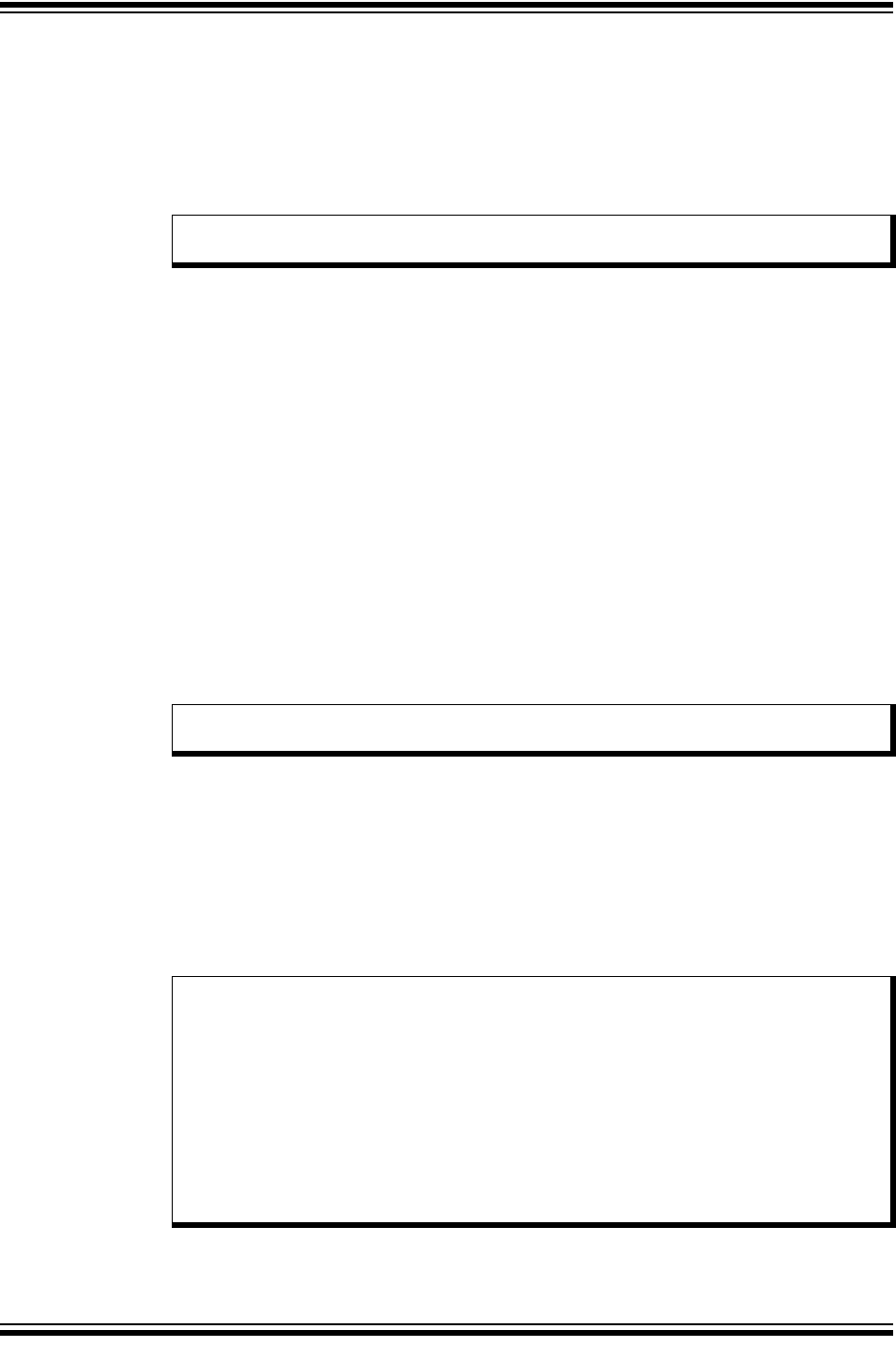
The transmitter block diagram of the UART module is illustrated in Figure 5-1. The important part
of the transmitter is the UARTx Transmit Shift Register (UxTSR). The Shift register obtains its
data from the transmit FIFO buffer, UxTXREG. The UxTXREG register is loaded with data in soft-
ware. The UxTSR register is not loaded until the Stop bit has been transmitted from the previous
load. As soon as the Stop bit is transmitted, the UxTSR is loaded with new data from the
UxTXREG register (if available).
Figure 5-1: UARTx Transmitter Block Diagram
The transmission is enabled by setting the UTXEN enable bit (UxSTA<10>). The actual trans-
mission will not occur until the UxTXREG register has been loaded with data and the Baud Rate
Generator (UxBRG) has produced a shift clock (Figure 5-1). Normally, when the first transmis-
sion is started, the UxTSR register is empty, so a transfer to the UxTXREG register will result in
an immediate transfer to UxTSR. Clearing the UTXEN bit during a transmission will cause the
transmission to be aborted and will reset the transmitter. As a result, the UxTX pin will revert to
a high-impedance state.
To select 9-bit transmission, the PDSEL<1:0> bits (UxMODE<2:1>) should be set to ‘11’ and the
ninth bit should be written to the UTX8 bit (UxTXREG<8>). A word write should be performed to
UxTXREG, so that all nine bits are written at the same time.
Note: The UxTSR register is not mapped in data memory, so it is not available to the user
application.
Word Write-Only
Word or
UTX8 UxTXREG Low Byte
Load UxTSR
Transmit Control
– Control UxTSR
– Control Buffer
– Generate Flags
– Generate Interrupt
UxTXIF
Data
(Start)
(Stop)
Parity
Parity
Generator
Transmit Shift Register (UxTSR)
Control
Signals
16x Baud Clock
from Baud Rate
Generator
Internal Data Bus
UTXBRK
Note: ‘x’ denotes the UART number.
UxTX
UxMODE
UxSTA
16
Byte Write
Transmit FIFO
15 9 8 7 0
UxCTS
UTXINV
16 Divider
Note: There is no parity in case of a 9-bit data transmission.

dsPIC33/PIC24 Family Reference Manual
DS70000582E-page 16 2009-2013 Microchip Technology Inc.
On a device Reset, the UxTX pin is configured as an input; therefore, the state of the UxTX pin
is undefined. When the UART module is enabled, the transmit pin is driven high. It remains in
this state until data is written to the transmit buffer (UxTXREG). The transmit pin is driven low as
soon as the first data is written to the UxTXREG register. To ensure the Start bit detection, it is
recommended to have a delay between enabling the UARTx (UARTEN = 1) and initiating the first
transmission. The delay is baud rate dependent and should be equal to, or longer than, the time
it takes to transmit one data bit.
Figure 5-2: UARTx Transmission
5.1 Transmit Buffer (UxTXREG)
The transmit buffer is 9 bits wide and 4 levels deep. Along with the UARTx Transmit Shift Register
(UxTSR), the user effectively has a 5-level deep buffer. It is organized as a First-In First-Out
(FIFO). Once the UxTXREG contents are transferred to the UxTSR register, the current buffer
location becomes available for new data to be written and the next buffer location is sourced to
the UxTSR register. The UTXBF (UxSTA<9>) status bit is set whenever the buffer is full. If a user
application attempts to write to a full buffer, the new data will not be accepted into the FIFO.
The FIFO is reset during any device Reset, but is not affected when the device enters a power-saving
mode or wakes up from a power-saving mode.
5.2 Transmit Interrupt
The UARTx Transmit Interrupt Flag bit (UxTXIF) is located in the corresponding Interrupt Flag
Status (IFS) register. The UTXISEL<1:0> control bits (UxSTA<15,13>) determine when the
UART will generate a transmit interrupt.
• If UTXISEL<1:0> = 00, the UxTXIF bit is set when a character is transferred from the
transmit buffer to the UARTx Transmit Shift Register (UxTSR) or the transmit buffer is
empty. This implies at least one location is empty in the transmit buffer.
• If UTXISEL<1:0> = 01, the UxTXIF bit is set when the last character is shifted out of the
UxTSR register. This implies that all the transmit operations are completed.
• If UTXISEL<1:0> = 10, the UxTXIF bit is set when the character is transferred to the
UxTSR register and the transmit buffer is empty.
The UxTXIF bit is set when the module is first enabled. The user application should clear the
UxTXIF bit in the Interrupt Service Routine (ISR).
Switching between the two interrupt modes during operation is possible.
While the UxTXIF flag bit indicates the status of the UxTXREG register, the TRMT bit
(UxSTA<8>) indicates the status of the UxTSR. The TRMT status bit is a read-only bit, which is
set when the UxTSR is empty. No interrupt logic is tied to this bit, so the user application has to
poll this bit to determine if the UxTSR is empty.
Note: When the UTXEN bit is set, the UxTXIF flag bit will also be set regardless of the
UTXISEL bits (UxSTA<15,13>) settings.
UxTX
1 2
B0 B1 B2 B3 B4 B5 B6 B7
Bit Time = T
Software
Delay
1. The UARTx module is enabled (UARTEN = 1).
2. Data is written to the transmit buffer (UxTXREG) to begin the transmission.

2009-2013 Microchip Technology Inc. DS70000582E-page 17
UART
5.3 Setup for UART Transmit
The following steps are used to set up a transmission:
1. Initialize the UxBRG register for the appropriate baud rate (see Section 3.0 “UART Baud
Rate Generator”).
2. Set the number of data bits, number of Stop bits and parity selection by writing to the
PDSEL<1:0> (UxMODE<2:1>) and STSEL (UxMODE<0>) bits.
3. If transmit interrupts are desired, set the UxTXIE control bit in the corresponding Interrupt
Enable Control x register (IECx).
4. Specify the interrupt priority for the transmit interrupt using the UxTXIP<2:0> control bits in
the corresponding Interrupt Priority Control x register (IPCx). Also, select the Transmit
Interrupt mode by writing to the UTXISEL<1:0> bits (UxSTA<15,13>).
5. Enable the UART module by setting the UARTEN bit (UxMODE<15>).
6. Enable the transmission by setting the UTXEN bit (UxSTA<10>), which also sets the UxTXIF bit.
7. The UxTXIF bit should be cleared in the software routine that services the UART transmit
interrupt. The operation of the UxTXIF bit is controlled by the UTXISEL<1:0> control bits.
8. Load data into the UxTXREG register (starts transmission).
If 9-bit transmission has been selected, load a word. If 8-bit transmission is used, load a
byte. Data can be loaded into the buffer until the UTXBF status bit (UxSTA<9>) is set.
Example 5-1 provides the sample code that sets up the UART for transmission.
Figure 5-3: UARTx Transmission (8-Bit or 9-Bit Data)
Figure 5-4: UARTx Transmission (Back-to-Back)
Note: The UTXEN bit should not be set until the UARTEN bit has been set; otherwise,
UART transmissions will not be enabled. Writing data to the UxTXREG should be
done after the UTXEN bit is set.
Character 1
Stop bit
Character 1 to
Transmit Shift Register
Start bit bit 0 bit 1 bit 7/8
Write to UxTXREG
BCLKx/16
(Shift Clock)
UxTX
UxTXIF
TRMT bit
Character 1
UxTXIF Cleared by User in Software
Transmit Shift Register
Write to UxTXREG
BCLKx/16
(Shift Clock)
UxTX
UxTXIF
TRMT bit
Character 1 Character 2
Character 1 to Character 2 to
Start bit Stop bit Start bit
Transmit Shift Register
Character 1 Character 2
bit 0 bit 1 bit 7/8 bit 0
Note: This timing diagram shows two consecutive transmissions.
(UTXISEL<1:0> =
00
)
UxTXIF
(UTXISEL<1:0> =
10
)
UxTXIF Cleared by User in Software

dsPIC33/PIC24 Family Reference Manual
DS70000582E-page 18 2009-2013 Microchip Technology Inc.
Example 5-1: UART1 Transmission with Interrupts
#define FP 40000000
#define BAUDRATE 9600
#define BRGVAL ((FP/BAUDRATE)/16)-1
unsigned int i;
#define DELAY_105uS asm volatile ("REPEAT, #4201"); Nop(); // 105uS delay
int main(void)
{
// Configure oscillator as needed
.
.
.
// Configure oscillator as needed
U1MODEbits.STSEL = 0; // 1-Stop bit
U1MODEbits.PDSEL = 0; // No Parity, 8-Data bits
U1MODEbits.ABAUD = 0; // Auto-Baud disabled
U1MODEbits.BRGH = 0; // Standard-Speed mode
U1BRG = BRGVAL; // Baud Rate setting for 9600
U1STAbits.UTXISEL0 = 0; // Interrupt after one TX character is transmitted
U1STAbits.UTXISEL1 = 0;
IEC0bits.U1TXIE = 1; // Enable UART TX interrupt
U1MODEbits.UARTEN = 1; // Enable UART
U1STAbits.UTXEN = 1; // Enable UART TX
/* Wait at least 105 microseconds (1/9600) before sending first char */
DELAY_105uS
U1TXREG = 'a'; // Transmit one character
while(1)
{
}
}
void __attribute__((__interrupt__)) _U1TXInterrupt(void)
{
IFS0bits.U1TXIF = 0; // Clear TX Interrupt flag
U1TXREG = 'a'; // Transmit one character
}

2009-2013 Microchip Technology Inc. DS70000582E-page 19
UART
5.4 Transmission of Break Characters
A Break character transmit consists of a Start bit, followed by twelve bits of ‘0’ and a Stop bit. A
Frame Break character is sent whenever the UTXBRK and UTXEN bits are set, while the
Transmit Shift Register is loaded with data. A dummy write to the UxTXREG register is necessary
to initiate the Break character transmission. Note that the data value written to the UxTXREG for
the Break character is ignored. The write simply serves the purpose of initiating the proper
sequence – all ‘0’s will be transmitted.
The UTXBRK bit is automatically reset by hardware after the corresponding Stop bit is sent. This
allows the user application to preload the transmit FIFO with the next transmit byte, following the
Break character (typically, the Sync character in the LIN/J2602 specification).
The TRMT bit indicates when the Transmit Shift Register is empty or full, just as it does during
the normal transmission. See Figure 5-5 for the timing of the Break character sequence.
Figure 5-5: Send Break Character Sequence
5.4.1 BREAK AND SYNC TRANSMIT SEQUENCE
The following sequence sends a message frame header made up of a Break, followed by an
auto-baud Sync byte. This sequence is typical of a LIN/J2602 bus master.
1. Configure the UART for the desired mode.
2. Set the UTXEN and UTXBRK bits to transmit the Break character.
3. Load the UxTXREG with a dummy character to initiate transmission (value is ignored).
4. Write 0x55 to UxTXREG – loads the Sync character into the transmit FIFO.
After the Break has been sent, the UTXBRK bit is reset by hardware. The Sync character is now
transmitted.
Note: The user application should wait for the transmitter to be Idle (TRMT = 1) before set-
ting the UTXBRK bit. The UTXBRK bit overrides any other transmitter activity. If the
user application clears the TXBRK bit prior to sequence completion, unexpected
module behavior can result. Sending a Break character does not generate a
transmit interrupt.
Write to UxTXREG
Start bit bit 0 bit 1 bit 11 Stop bit
Break
UxTX
TRMT bit
UTXBRK Sampled Here
Auto-Cleared
UTXBRK bit
UxTXIF
BCLKx/16
(Shift Clock)
Dummy Write

dsPIC33/PIC24 Family Reference Manual
DS70000582E-page 20 2009-2013 Microchip Technology Inc.
6.0 DATA BIT DETECTION
6.1 16X Clock Mode (BRGH = 0)
In 16x Clock mode, each bit of the received data is 16 clock pulses wide. To detect the value of
an incoming data bit, the bit is sampled at the 7th, 8th and 9th rising edges of the clock. These
rising edges are called Majority Detection edges. This mode is more robust than 4x Clock mode.
Figure 6-1: 16x Clock Mode with Majority Detection
6.2 4X Clock Mode (BRGH = 1)
In 4x Clock mode, each bit of the received data is four clock pulses wide. The 4x Clock mode
does not provide enough edges to support the Majority Detection method. Therefore, the
received data is sampled at the one-half bit width.
Figure 6-2: 4x Clock Mode without Majority Detection
Note: In 16x Clock mode, each bit is sampled at 7th, 8th and 9th rising edges of the clock.
Idle Start bit bit 0
MD2
MD3
MD1
Start Bit Detected
16x Clock
Bit Clock
Internal Bit Counter
(Received Data)
Start bit bit 0 bit 1
Sample Point
4x Clock
Bit Clock
Internal Bit Counter
RX
Note: In 4x Clock mode, the sampling occurs only at the one-half bit width.
2009-2013 Microchip Technology Inc. DS70000582E-page 21
UART
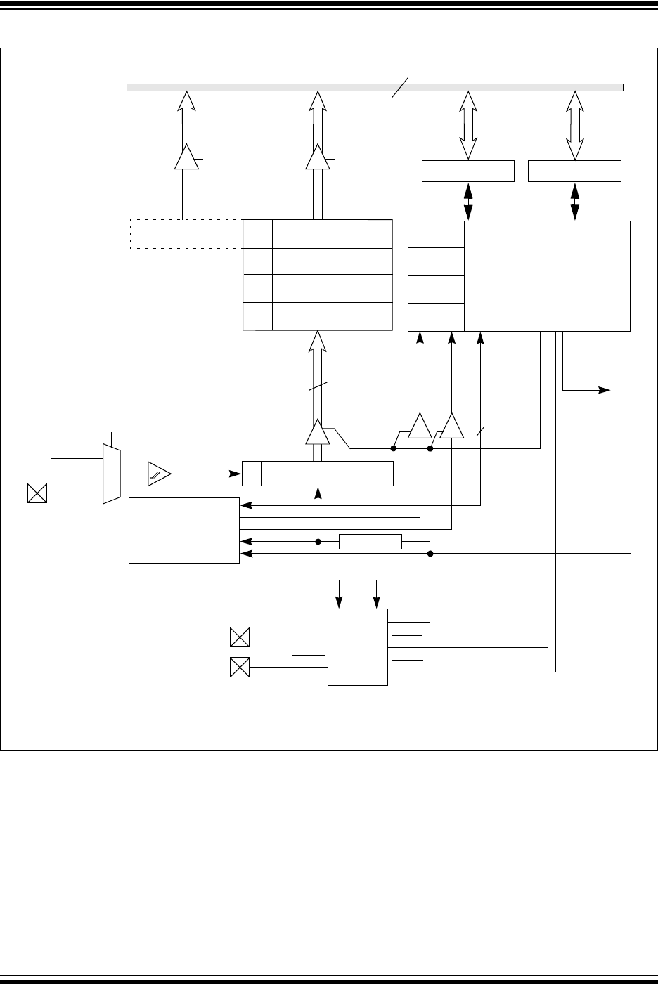
7.0 UART RECEIVER
The receiver block diagram of the UART module is illustrated in Figure 7-1. The important part
of the receiver is the UARTx Receive (Serial) Shift Register (UxRSR). The data is received on
the UxRX pin and is sent to the data recovery block. After sampling the UxRX pin for the Stop bit,
the received data in the UxRSR register is transferred to the receive FIFO (if it is empty). The
data recovery block operates at 16 times the baud rate, whereas the main receive serial shifter
operates at the baud rate.
The data on the UxRX pin is sampled multiple times by a Majority Detect circuit to determine if a
high or a low level is present at the UxRX pin.
7.1 Receive Buffer (UxRXREG)
The UART receiver has a 4 deep, 9-bit wide FIFO receive data buffer. The UxRXREG is a
memory mapped register that provides access to the output of the FIFO. It is possible for four
words of data to be received and transferred to the FIFO, and a fifth word to begin shifting to the
UxRSR register before a buffer overrun occurs.
7.2 Receiver Error Handling
If the FIFO is full (four characters) and a fifth character is fully received into the UxRSR register,
the OERR bit (UxSTA<1>) will be set. The word in the UxRSR register will be kept, but further
transfers to the receive FIFO and UART interrupts are inhibited as long as the OERR bit is set.
The user application must clear the OERR bit in software to allow further data to be received.
If it is desired to keep the data received prior to the overrun, the user application should first read
all five characters, then clear the OERR bit. If the five characters can be discarded, the user
application can simply clear the OERR bit. This effectively resets the receive FIFO and all prior
received data is lost.
The Framing Error bit, FERR (UxSTA<2>), is set if a Stop bit is detected at a logic low level.
The Parity Error bit, PERR (UxSTA<3>), is set if a parity error has been detected in the data word
at the top of the buffer (i.e., the current word). For example, a parity error would occur if the parity
is set to be even, but the total number of ‘1’s in the data has been detected to be odd. The PERR
bit is irrelevant in 9-bit mode. The FERR and PERR bits are buffered along with the
corresponding word and should be read before reading the data word.
An interrupt is generated if any of these (OERR, FERR and PERR) errors occur. The user
application needs to enable the corresponding UARTx Interrupt Enable Control bit (UxERIE) in
the IECx register to go to the corresponding interrupt vector location.
Note: The UxRSR register is not mapped in the data memory, so it is not available to the
user application.
Note: The data in the receive FIFO should be read prior to clearing the OERR bit. The
FIFO is reset when OERR is cleared, which causes all data in the buffer to be lost.
Note: After a Reset, the three possible UART interrupts have the same Interrupt Priority
Level (IPL). Natural order allows the (RX/TX) data interrupts to be serviced before
the UART error interrupt.
To allow the UART error interrupt to be serviced before the (RX/TX) data interrupts,
its Interrupt Priority Level (UxEIP) is raised or the data Interrupt Priority Levels are
lowered (UxRXIP and UxTXIP).
Example for UART2 to raise the UART2 error interrupt level:
• IPC7bits.U2RXIP = 4; //UART2 RX interrupt priority, mid-range
• IPC7bits.U2TXIP = 4; //UART2 TX interrupt priority, mid-range
• IPC16bits.U2EIP = 5; //UART2 error priority set higher

dsPIC33/PIC24 Family Reference Manual
DS70000582E-page 22 2009-2013 Microchip Technology Inc.
7.3 Receive Interrupt
The UARTx Receive Interrupt Flag (UxRXIF) bit is located in the corresponding Interrupt Flag
Status x register (IFSx). The URXISEL<1:0> control bits (UxSTA<7:6>) determine when the
UART receiver generates an interrupt.
• If URXISEL<1:0> = 00 or 01, an interrupt is generated each time a data word is transferred
from the UARTx Receive Shift Register (UxRSR) to the receive buffer. There may be one or
more characters in the receive buffer.
• If URXISEL<1:0> = 10, an interrupt is generated when a word is transferred from the
UxRSR register to the receive buffer, and as a result, the receive buffer contains three or
four characters.
• If URXISEL<1:0> = 11, an interrupt is generated when a word is transferred from the
UxRSR register to the receive buffer, and as a result, the receive buffer contains four
characters (i.e., becomes full).
Switching between the three Interrupt modes during operation is possible.
While the URXDA and UxRXIF flag bits indicate the status of the UxRXREG register, the RIDLE
bit (UxSTA<4>) shows the status of the UxRSR register. The RIDLE status bit is a read-only bit
and is set when the receiver is Idle (i.e., the UxRSR register is empty). No interrupt logic is tied
to this bit, so the user application needs to poll this bit in order to determine if the UxRSR register
is Idle.
The URXDA bit (UxSTA<0>) is a read-only bit, which indicates whether the receive buffer has
data or is empty. This bit is set as long as there is at least one character to be read from the
receive buffer.
Figure 7-1 illustrates a block diagram of the UART receiver.
2009-2013 Microchip Technology Inc. DS70000582E-page 23
UART
Figure 7-1: UARTx Receiver Block Diagram
URX8 UxRXREG Low Byte
Load UxRSR
UxMODE
Receive Buffer Control
– Generate Flags
– Generate Interrupt
UxRXIF
UxRX
• Start bit Detect
Receive Shift Register
Control
Signals
16x Baud Clock
from Baud Rate
Generator
UxSTA
– Shift Data Characters
to Buffer
9
(UxRSR)
PERR
FERR
• Parity Check
• Stop bit Detect
• Shift Clock Generation
• Wake Logic
16
Internal Data Bus
1
0
LPBACK
From UxTX
15 9 8 7 0
Word Word or
Byte Read
BCLKx/UxRTS
UxCTS
Selection
UEN
BCLKx
UEN1
UEN0
16 Divider
UxRTS
UxCTS
Note: The ‘x’ denotes the UART number.
Read-Only
dsPIC33/PIC24 Family Reference Manual
DS70000582E-page 24 2009-2013 Microchip Technology Inc.
7.4 Setup for UART Reception
The following steps are used to set up a UART reception:
1. Initialize the UxBRG register for the appropriate baud rate (see Section 3.0 “UART Baud
Rate Generator”).
2. Set the number of data bits, number of Stop bits and parity selection by writing to the
PDSEL<1:0> (UxMODE<2:1>) and STSEL (UxMODE<0>) bits.
3. If interrupts are desired, set the UxRXIE bit in the corresponding Interrupt Enable
Control x register (IECx).
Specify the interrupt priority for the interrupt using the UxRXIP<2:0> control bits in the cor-
responding Interrupt Priority Control x register (IPCx). Also, select the Receive Interrupt
mode by writing to the URXISEL<1:0> bits (UxSTA<7:6>).
4. Enable the UART module by setting the UARTEN bit (UxMODE<15>).
5. Receive interrupts will depend on the URXISEL<1:0> control bit settings.
If receive interrupts are not enabled, the user application can poll the URXDA bit. The
UxRXIF bit should be cleared in the software routine that services the UART receive
interrupt.
6. Read data from the receive buffer.
If 9-bit transmission is selected, read a word; otherwise, read a byte. The URXDA status
bit (UxSTA<0>) is set whenever the data is available in the buffer.
Example 7-1 provides the sample code that sets up the UART for reception.
Figure 7-2: UARTx Reception
(1,2)
Figure 7-3: UARTx Reception with Receive Overrun
Start
bit bit 1bit 0 bit 7 bit 0Stop
bit
Start
bit bit 7 Stop
bit
UxRX
RIDLE bit
Character 1
to UxRXREG
Character 2
to UxRXREG
UxRXIF
(URXISEL<1:0> =
0x
)
Note 1: This timing diagram shows two characters received on the UxRX input.
2: If the interrupt flag is used by the application software as a basis for disabling the UART transmission, the software should
wait for 1-bit time before disabling the transmission.
Start
bit bit 7/8bit 1bit 0 bit 7/8 bit 0Stop
bit
Start
bit
Start
bitbit 7/8 Stop
bit
UxRX
OERR bit
RIDLE bit
Characters 1, 2, 3 and 4
Stored in Receive FIFO
Character 5
Held in UxRSR
Stop
bit
Character 1 Characters 2, 3, 4 and 5 Character 6
OERR Cleared by User in Software
Note: This diagram shows 6 characters received without the user reading the input buffer. The 5th character received is held in the
Receive Shift register. An overrun error occurs at the start of the 6th character.

2009-2013 Microchip Technology Inc. DS70000582E-page 25
UART
Example 7-1: UART1 Receive Only with Polling (Interrupts Disabled)
#define FP 40000000
#define BAUDRATE 9600
#define BRGVAL ((FP/BAUD RATE)/16) - 1
int main(void)
{
// Configure oscillator as needed
.
.
.
// Configure oscillator as needed
U1MODEbits.STSEL = 0; // 1-stop bit
U1MODEbits.PDSEL = 0; // No Parity, 8-data bits
U1MODEbits.ABAUD = 0; // Auto-Baud disabled
U1MODEbits.BRGH = 0; // Standard-Speed mode
U1BRG = BRGVAL; // Baud Rate setting for 9600
U1STAbits.URXISEL = 0; // Interrupt after one RX character is received;
U1MODEbits.UARTEN = 1; // Enable UART
while(1)
{
char ReceivedChar;
/* Check for receive errors */
if(U1STAbits.FERR == 1)
{
continue;
}
/* Must clear the overrun error to keep UART receiving */
if(U1STAbits.OERR == 1)
{
U1STAbits.OERR = 0;
continue;
}
/* Get the data */
if(U1STAbits.URXDA == 1)
{
ReceivedChar = U1RXREG;
}
}

dsPIC33/PIC24 Family Reference Manual
DS70000582E-page 26 2009-2013 Microchip Technology Inc.
8.0 USING THE UART FOR 9-BIT COMMUNICATION
The UART receiver can be used in 9-Bit Data mode for multiprocessor communication. With the
ADDEN bit set in 9-Bit Data mode, the receiver can ignore the data when the 9th bit of the data
is ‘0’. This feature can be used in a multiprocessor environment.
8.1 Multiprocessor Communications
A typical multiprocessor communication protocol will differentiate between the data bytes and the
address/control bytes. A common scheme is to use a 9th data bit to identify whether a data byte
is address or data information. If the 9th bit is set, the data is processed as address or control
information. If the 9th bit is cleared, the received data word is processed as data associated with
the previous address/control byte.
The protocol operates as follows:
• The master device transmits a data word with the 9th bit set. The data word contains the
address of a slave device.
• All slave devices in the communication chain receive the address word and check the slave
address value.
• The slave device that was addressed will receive and process subsequent data bytes sent
by the master device. All other slave devices will discard subsequent data bytes until a new
address word (9th bit set) is received.
8.2 ADDEN Control Bit
The UART receiver has an Address Detect mode, which allows it to ignore data words with the
9th bit cleared. This reduces the interrupt overhead because the data words with the 9th bit
cleared are not buffered. This feature is enabled by setting the ADDEN bit (UxSTA<5>).
The UART must be configured for 9-bit Data mode to use the Address Detect mode. The ADDEN
bit has no effect when the receiver is configured in 8-bit Data mode.
8.3 Setup for 9-Bit Transmit
The setup procedure for 9-bit transmission is identical to the procedure for 8-Bit Transmit modes,
except that the PDSEL<1:0> bits (UxMODE<2:1>) should be set to ‘11’ (see Section 5.3 “Setup
for UART Transmit”).
Word writes should be performed to the UxTXREG register (starts transmission).

2009-2013 Microchip Technology Inc. DS70000582E-page 27
UART
8.4 Setup for 9-Bit Reception Using Address Detect Mode
The setup procedure for 9-bit reception is similar to the procedure for 8-Bit Receive modes,
except that the PDSEL<1:0> bits (UxMODE<2:1>) should be set to ‘11’ (see Section 7.4 “Setup
for UART Reception”).
The Receive Interrupt mode should be configured by writing to the URXISEL<1:0>
(UxSTA<7:6>) bits.
The procedure for using the Address Detect mode is as follows:
1. Set the ADDEN bit (UxSTA<5>) to enable address detect. Ensure that the URXISEL<1:0>
control bits are configured to generate an interrupt after each received word.
2. Check each 8-bit address by reading the UxRXREG register to determine if the device is
being addressed.
3. If this device has not been addressed, discard the received word.
4. If this device has been addressed, clear the ADDEN bit to allow subsequent data bytes to
be read into the receive buffer and interrupt the CPU.
If a long data packet is expected, the Receive Interrupt mode can be changed to buffer
more than one data byte between the interrupts.
5. After receiving the last data byte, set the ADDEN bit so that only address bytes are
received.
Also, ensure that the URXISELx control bits are configured to generate an interrupt after
each received word.
Figure 8-1: UARTx Reception with Address Detect (ADDEN = 1)
Note: If the Address Detect mode is enabled (ADDEN = 1), the URXISEL<1:0> control bits
should be configured so that an interrupt will be generated after every received
word. Each received data word must be checked in software for an address match
immediately after reception.
Start
bit bit 1bit 0 bit 8 bit 0Stop
bit
Start
bit bit 8 Stop
bit
UxRX (pin)
Read Rcv
Buffer Register
UxRXREG
UxRXIF
(Interrupt Flag)
Word 1
UxRXREG
bit 8 = 0, Data Byte bit 8 = 1, Address Byte
Transfer
to Receive FIFO
Note: This timing diagram shows a data byte followed by an address byte. The data byte is not read into the UxRXREG (receive buffer)
because ADDEN = 1 and bit 8 = 0.

dsPIC33/PIC24 Family Reference Manual
DS70000582E-page 28 2009-2013 Microchip Technology Inc.
8.5 Address Match Detect
The UART has a built-in feature that can perform address match detection to off-load this task from
the processors. The ADM_ADD<7:0> (UxADMD<7:0>) address and ADM_MASK<7:0>
(UxADMD<15:8>) address mask bits are used to hold the desired address and mask bits, respec-
tively. If ADDEN = 1 and the 9th bit received is a ‘1’, the data in the Receive Shift register is
compared to the ADM_ADDx bits and masked with the ADM_MASKx bits. If a match is found, the
data is transferred from the Receive Shift register to the UxRXBUF according to Table 8-1.
If an address match is found, software must clear ADDEN = 0 to receive the remainder of the
message; interrupts on the body of the message will occur as specified by URXISEL<1:0>
(UxSTA<7:6>). After the body of the message is received, software must set ADDEN = 1 to
enable Address Detect mode once again.
8.5.1 USING ADDRESS MATCH DETECT
The setup procedure for 9-bit reception is similar to the procedure for 8-Bit Receive modes,
except that the PDSEL<1:0> bits (UxMODE<2:1>) should be set to ‘11’ (see Section 7.4 “Setup
for UART Reception”).
1. Write the desired match address to ADM_ADDR<7:0>.
2. Write the desired address mask to ADM_MASK<7:0>.
3. Set PDSEL<1:0> = 11 to choose 9-bit mode.
4. Set ADDEN = 1 to enable automatic address detection.
5. When an interrupt is received, the matching address will be stored in the UxRXBUF. If a
mask is being used for decision logic, user software can read it from UxRXBUF. If the
address is not needed, it should be cleared from the buffer with a dummy read.
6. Clear ADDEN to allow the reception of the following data. Interrupts on the body of the
message will occur as specified by URXISEL<1:0>.
7. When reception of the body of message is completed (as determined in the application
software), set the ADDEN bit to ‘1’ to detect the next message address.
Note: Not all devices support address match detect. Refer to the specific device data
sheet for availability.
Table 8-1: Address Match Detection
Condition Action
(UxRSR<7:0> and ADM_MASK<7:0>) = (ADM_ADDR<7:0>
and ADM_MASK<7:0>)
(1)
UxBUF = UxRSR<7:0>
(UxRSR<7:0> and ADM_MASK<7:0>) ≠ (ADM_ADDR<7:0>
and ADM_MASK<7:0>)
(1)
None, UxRSR will be
overwritten with next
incoming byte
Note 1: ADM_MASKx bits set to ‘0’ are regarded as ‘don’t care’ for that address bit position.
Note: The URXISEL<1:0> control bits do not have any impact on the interrupt generation
in this mode. If the 9th bit is a ‘1’, an interrupt is generated, regardless of the state
of the URXISEL<1:0> bits.

2009-2013 Microchip Technology Inc. DS70000582E-page 29
UART
9.0 OTHER FEATURES OF THE UART
9.1 UART in Loopback Mode
Setting the LPBACK bit (UxMODE<6>) enables the Loopback mode, in which the UxTX output
is internally connected to the UxRX input. When configured for the Loopback mode, the UxRX
pin is disconnected from the internal UART receive logic. However, the UxTX pin still functions
normally.
To select Loopback mode, follow these steps:
1. Configure the UART module for the desired mode of operation.
2. Enable transmission as defined in Section 5.0 “UART Transmitter”.
3. Set the LPBACK bit = 1 to enable Loopback mode.
The Loopback mode is dependent on the UEN<1:0> bits, as shown in Tab l e 9-1.
Table 9-1: Loopback Mode Pin Function
9.2 Auto-Baud Support
To allow the system to determine baud rates of the received characters, the ABAUD bit
(UxMODE<5>) is enabled. The UART begins an automatic baud rate measurement sequence
whenever a Start bit is received while the Auto-Baud Rate Detect is enabled (ABAUD = 1). The
calculation is self-averaging. Once the ABAUD bit is set, the BRG counter value will be cleared
and will look for a Start bit, which in this case, is defined as a high-to-low transition, followed by
a low-to-high transition.
Following the Start bit, the auto-baud expects to receive an ASCII “U” (“55h”) in order to
calculate the proper bit rate. The measurement is taken over both the low and the high bit time
in order to minimize any effects caused by asymmetry of the incoming signal. On the 5th UxRX
pin rising edge, an accumulated BRG counter value, totaling the proper BRG period, is
transferred to the UxBRG register. The ABAUD bit is automatically cleared. If the user
application clears the ABAUD bit prior to sequence completion, unexpected module behavior
can result. See Figure 9-1 for the Auto-Baud Rate Detection sequence.
UEN<1:0>
Pin Function, LPBACK = 1
(1)
00 UxRX input connected to UxTX; UxTX pin functions; UxRX pin ignored; UxCTS/
UxRTS
unused
01 UxRX input connected to UxTX; UxTX pin functions; UxRX pin ignored;
UxRTS
pin functions; UxCTS unused
10 UxRX input connected to UxTX; UxTX pin functions; UxRX pin ignored;
UxRTS
pin functions; UxCTS input connected to UxRTS; UxCTS pin ignored
11 UxRX input connected to UxTX; UxTX pin functions; UxRX pin ignored;
BCLKx pin functions; UxCTS
/UxRTS unused
Note 1: The LPBACK bit should be set to ‘1’ only after enabling the other bits associated
with the UART module.
Note: Depending on the specific device used, the ABAUD feature of a respective UART
may automatically use the corresponding Input Capture x (ICx) peripheral for
UARTx auto-baud measurements. For devices that use the corresponding ICx
peripheral, the user application should not use the respective ICx peripheral for
other purposes. See the specific device data sheet regarding this dependency.

dsPIC33/PIC24 Family Reference Manual
DS70000582E-page 30 2009-2013 Microchip Technology Inc.
Figure 9-1: Automatic Baud Rate Calculation
While the auto-baud sequence is in progress, the UART state machine is held in an Idle state.
The UxRXIF interrupt is set on the 5th UxRX rising edge, independent of the URXISEL<1:0> bits
setting. The receiver FIFO is not updated.
BRG Counter
UxRX
ABAUD bit
bit 0 bit 1
BRG Clock
Start
Auto-Cleared
Set by User Software
XXXXh 0000h
Edge 1
bit 2 bit 3
Edge 2
bit 4 bit 5
Edge 3
bit 6 bit 7
Edge 4
Stop bit
Edge 5
001Ch
BRG Register
XXXXh 001Ch
UxRXIF

2009-2013 Microchip Technology Inc. DS70000582E-page 31
UART
10.0 UART OPERATION WITH DMA
On some dsPIC33 and PIC24 devices, the Direct Memory Access (DMA) module can be used
to transfer data between the CPU and UART without CPU assistance. Refer to the specific
device data sheet to see if DMA is present on your particular device. For more information on the
DMA module, refer to the Direct Memory Access (DMA) FRM that pertains to the specific device
being used.
10.1 UART Receive with DMA
If the DMA channel is associated with the UART receiver, the UART should issue a DMA request
every time there is a character ready to be moved from the UART module to RAM. The DMA
transfers data from the UxRXREG register into RAM and issues a CPU interrupt after a pre-
defined number of transfers. As the DMA channels are unidirectional, the UART receive
operation would require one DMA channel.
The UART module must be configured to generate interrupts for every character received. For
the UART receiver to generate an RX interrupt for each character received, the UART Receive
Interrupt Mode Selection bits (URXISEL<1:0>) must be set to ‘00’ or ‘01’ in the Status and Con-
trol register (UxSTA). When the UART and DMA channel are properly configured, the UART
receiver issues a DMA request as soon as data is received. No special steps need to be taken
by the user application to initiate a DMA transfer.
While configuring for UART reception, the word size of the DMA channel should be set to 16-bit.
This configures the DMA channel to read 16 bits from the UART module when data is available to
be read. The lower byte of the data represents the actual data byte received by the UART module.
The upper byte contains the UART status when the byte was received. Note that the reading of the
UxSTA register, when the UART reception is DMA enabled, will not return the status of the FERR
and PERR bits. This status is available in the upper byte of the 16-bit word that the DMA channel
transfers from the UART module to DMA RAM. Figure 10-1 illustrates the organization of the 16-bit
word transferred by DMA from the UART module to the DMA RAM.
Figure 10-1: Format of 16-Bit UART Receive Data Word Transferred by DMA to RAM
The UARTx Error Interrupt Flag bit (UxEIF) gets set if the last UART reception caused a framing
or a parity error. Setting the UxEIE bit causes the CPU to enter the UART error Interrupt Service
Routine (ISR). The user application can then inspect the upper byte of the last transferred word
to check which error condition has caused the interrupt.
—
12 10 9 bit 0711bit 15 8
Received UART Byte—FERR—PERR

dsPIC33/PIC24 Family Reference Manual
DS70000582E-page 32 2009-2013 Microchip Technology Inc.
10.2 UART Transmit with DMA
If the DMA channel is associated with the UART transmitter, the UART issues a DMA request
after each successful transmission. After each DMA request, the DMA transfers new data into
the UxTXREG register and issues a CPU interrupt after a predefined number of transfers. As the
DMA channels are unidirectional, one DMA channel is required for transmit.
In addition, the UART must be configured to generate interrupts for every character transmitted.
For the UART transmitter to generate a TX interrupt for each character transmitted, the UART
Transmission Interrupt Mode Selection bits (UTXISEL0 and UTXISEL1) must be set to ‘0’ in the
UxSTA register.
The UART transmitter issues a DMA request as soon as the UART and transmitter are enabled.
This means that the DMA channel and buffers must be initialized and enabled before the UART
and transmitter are enabled.
Note: For PIC24H, PIC24EP and dsPIC
®
devices only, alternatively, the UART transmitter
can be enabled before the DMA channel is enabled. In this case, the UART trans-
mitter DMA request will be lost and the user application must issue a DMA request
to start DMA transfers by setting the FORCE bit in the DMAxREQ register.

2009-2013 Microchip Technology Inc. DS70000582E-page 33
UART
11.0 UART OPERATION DURING CPU SLEEP AND IDLE MODES
11.1 UART Operation in Sleep Mode
When the device enters Sleep mode, all clock sources supplied to the UART module are shut
down and stay at logic ‘0’. If the device enters Sleep mode in the middle of a UART transmission
or reception operation, the operation is aborted and the UARTx pins (BCLKx, UxRTS and UxTX)
are driven to the default state.
A Start bit, when detected on the UARTx Receive pin (UxRX), can wake up the device from Sleep
mode if the WAKE bit (UxMODE<7>) is set just before the device enters Sleep mode. In this
mode, if the UARTx Receive Interrupt (UxRXIE) is enabled, a falling edge on the UART receive
pin generates a UARTx Receive Interrupt Flag (UxRXIF).
The receive interrupt wakes up the device from Sleep and the following events occur:
• If the assigned priority for the interrupt is less than or equal to the current CPU priority, the
device wakes up and continues code execution from the instruction following the PWRSAV
instruction that initiated Sleep mode.
• If the assigned priority level for the interrupt source is greater than the current CPU priority,
the device wakes up and the CPU execution process begins. Code execution continues
from the first instruction of the captured ISR.
• The UART does not recognize the first character received after a wake from Sleep due to
the delay in restoration of the clocks after the oscillator restart.
The WAKE bit is automatically cleared when a low-to-high transition is observed on the UxRX
line following the wake-up event.
11.2 UART Operation in Idle Mode
• When the device enters Idle mode, the system clock sources remain functional, but the
CPU stops code execution. The UART Stop in Idle bit (USIDL) in the UARTx Mode register
(UxMODE<13>) determines whether the module stops in Idle mode or continues to operate
in Idle mode.
•If USIDL = 0, the module continues to operate in Idle mode and provides full functionality.
•If USIDL = 1, the module stops in Idle mode. The module performs the same functions
when stopped in Idle mode as in Sleep mode (refer to Section 11.1 “UART Operation in
Sleep Mode”).
11.3 Auto-Wake-up on Sync Break Character
The auto-wake-up feature is enabled with the WAKE bit (UxMODE<7>). Once WAKE is active,
the typical receive sequence on UxRX is disabled. Following the wake-up event, the module
generates the UxRXIF interrupt.
The LPBACK bit (UxMODE<6>) must equal ‘0’ for wake-up to operate.
A wake-up event consists of a high-to-low transition on the UxRX line. This coincides with the
start of a Sync Break or a Wake-up Signal character for the LIN/J2602 protocol. When WAKE is
active, the UxRX line is monitored independently from the CPU mode. The UxRXIF interrupt will
be generated synchronously to the Q clocks in normal user mode, and asynchronously, if the
module is disabled due to Sleep or Idle mode. To assure that no actual data is lost, the WAKE bit
should be set just prior to entering the Sleep mode and while the UART module is in Idle.
The WAKE bit is automatically cleared once a low-to-high transition is observed on the UxRX line
following the wake-up event. At this point, the UART module is in Idle mode and is returned to
normal operation. This signals to the user that the Sync Break event is over. If the user clears the
WAKE bit prior to sequence completion, unexpected module behavior can result.

dsPIC33/PIC24 Family Reference Manual
DS70000582E-page 34 2009-2013 Microchip Technology Inc.
The wake-up event causes a receive interrupt by setting the UxRXIF bit. The UARTx Receive
Interrupt Select mode bits (URXISEL<1:0>) are ignored for this function. If the UxRXIF interrupt
is enabled, then this will wake up the device.
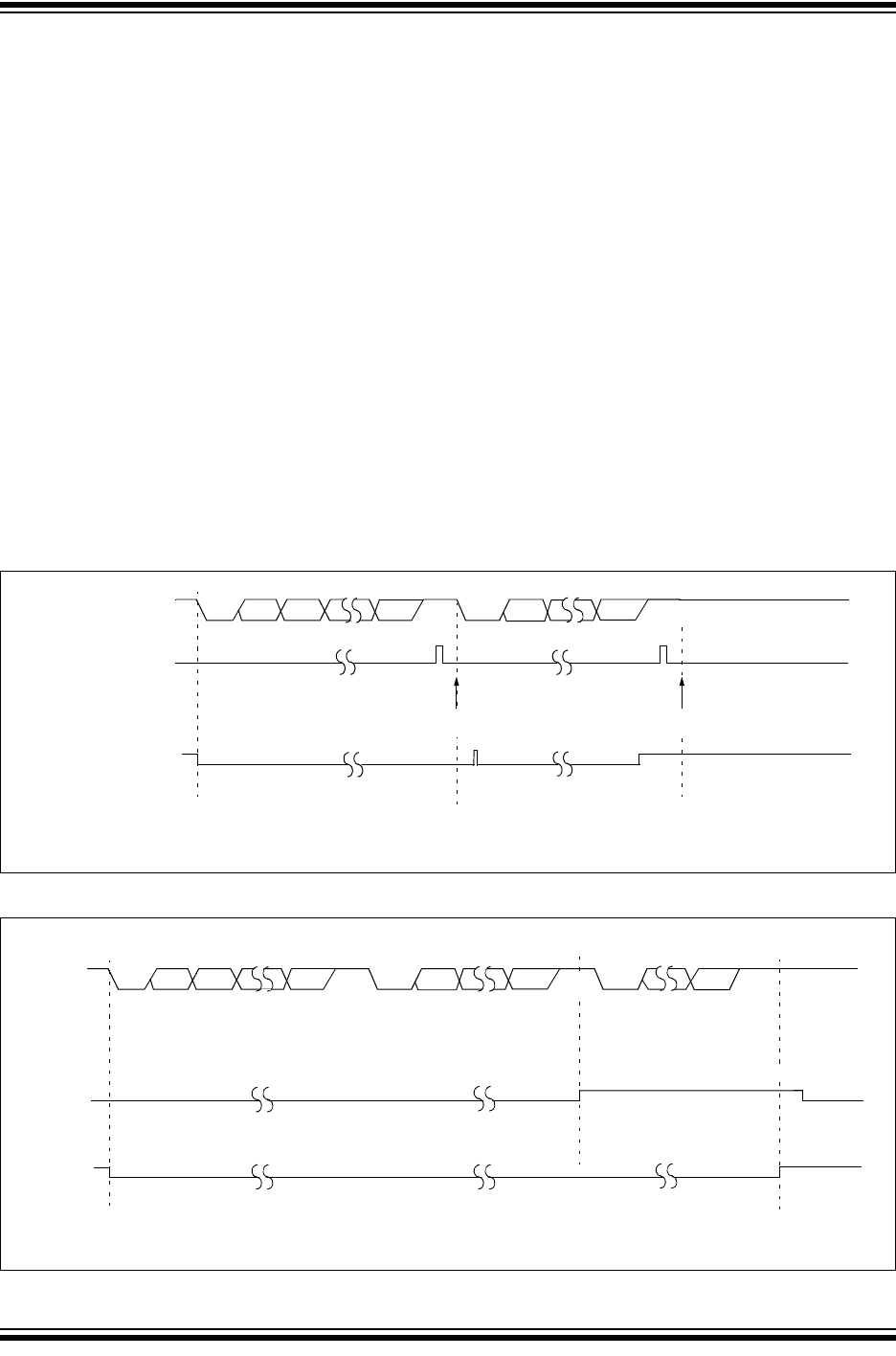
Figure 11-1: Auto-Wake-up Bit (WAKE) Timings During Normal Operation
Figure 11-2: Auto-Wake-up Bit (WAKE) Timings During Sleep
Note 1: The Sync Break (or Wake-up Signal) character must be of sufficient length to allow
enough time for the selected oscillator to start and provide proper initialization to
the UART. To ensure that the UART wakes up in time, the user application should
read the value of the WAKE bit (UxMODE<7>). If it is clear, it is possible that the
UART was not ready in time to receive the next character and the module might
need to be resynchronized to the bus.
2: In Sleep mode, a Start bit, when detected, causes the device to wake up only if the
WAKE bit (UxMODE<7>) is set just before the device enters Sleep mode.
3: In Sleep and Idle modes, as the falling edge on the UART receive pin generates a
UART receive interrupt, a dummy byte is copied if the UART receive buffer is read
in the first UART receive interrupt.
OSC1
WAKE bit
(1)
UxRX
UxRXIF
Note 1: UARTx state machine is held in Idle while WAKE bit is active.
Bit Set by User
Auto-Cleared
OSC1
WAKE bit
(2)
UxRX
UxRXIF
Sleep
Note 1: If the wake-up event requires a long oscillator warm-up time, the auto-clear of the WAKE bit can occur while the system
clocks are still active. This sequence should not depend on the presence of F
P.
2: The UARTx state machine is held in Idle while the WAKE bit is active.
(Note 1)
Bit Set by
Auto-Cleared
User Software

2009-2013 Microchip Technology Inc. DS70000582E-page 35
UART
12.0 OPERATION OF UxCTS AND UxRTS CONTROL PINS
The UxCTS (Clear-to-Send) and UxRTS (Request-to-Send) pins are the two hardware controlled
pins associated with the UART module. These two pins allow the UART to operate in Flow Con-
trol and Simplex modes, which are explained in detail in Section 12.2 “UxRTS Function in Flow
Control Mode” and Section 12.3 “UxRTS Function in Simplex Mode”, respectively. They are
implemented to control transmission and reception between the UART and Data Terminal
Equipment (DTE).
12.1 UxCTS Function
During UART operation, the UxCTS pin acts as an input pin, which can control the transmission.
This pin is controlled by another device (typically a PC). The UxCTS
pin is configured using the
UEN<1:0> bits (UxMODE<9:8>).
• When UEN<1:0> = 10, UxCTS is configured as an input.
• If UxCTS
= 1, the transmitter will go as far as loading the data in the Transmit Shift Register,
but will not initiate a transmission. This will allow the DTE to control and receive data from the
controller per its requirements.
The UxCTS
pin is sampled while the transmit data changes (i.e., at the beginning of the 16 baud
clocks). The transmission begins only when the UxCTS
is sampled low. The UxCTS is sampled
internally with a T
P, which means that there should be a minimum pulse width of 1 TP on UxCTS.
However, this cannot be a specification as the T
P can vary depending on the clock used.
The user application can also read the status of the UxCTS
by reading the associated port pin.
12.2 UxRTS Function in Flow Control Mode
During Flow Control mode, the UxRTS pin of one DTE is connected to the UxCTS pin of the
dsPIC33 or PIC24 device, and the UxCTS
pin of the DTE is connected to the UxRTS pin of the
device, as illustrated in Figure 12-1. The UxRTS
signal indicates that the device is ready to
receive the data. The UxRTS
pin is driven as an output whenever UEN<1:0> = 01 or 10. The
UxRTS
pin is asserted (driven low) whenever the receiver is ready to receive data. When the
RTSMD bit = 0 (when the device is in Flow Control mode), the UxRTS
pin is driven low whenever
the receive buffer is not full or the OERR bit is not set. When the RTSMD bit = 0, the UxRTS
pin
is driven high whenever the device is not ready to receive (i.e., when the receiver buffer is either
full or in the process of shifting).
Since the UxRTS
pin of the DTE is connected to the UxCTS pin of the dsPIC33 and PIC24
devices, the UxRTS
pin drives the UxCTS pin low whenever it is ready to receive the data. Trans-
mission of the data begins when the UxCTS
pin goes low, as explained in Section 12.1 “UxCTS
Function”.
12.3 UxRTS Function in Simplex Mode
During Simplex mode, the UxRTS pin of the DCE is connected to the UxRTS pin of the dsPIC33
or PIC24 device, and the UxCTS
pin of the DCE is connected to the UxCTS pin of the device, as
illustrated in Figure 12-2. In Simplex mode, the UxRTS
signal indicates that the DTE is ready to
transmit. The DCE replies to the UxRTS
signal with the valid UxCTS whenever the DCE is ready
to receive the transmission. When the DTE receives a valid UxCTS
signal, it will begin
transmission.
As illustrated in Figure 12-3, Simplex mode is also used in IEEE-485 systems to enable trans-
mitters. When UxRTS
indicates that the DTE is ready to transmit, the UxRTS signal enables the
driver.
Note: The UxCTS and UxRTS pins are not available on all devices. Refer to the “Universal
Asynchronous Receiver Transmitter (UART)” chapter of the specific device data
sheet for availability.

dsPIC33/PIC24 Family Reference Manual
DS70000582E-page 36 2009-2013 Microchip Technology Inc.
The UxRTS pin is configured as an output and is driven whenever UEN<1:0> = 01 or 10. When
RTSMD = 1, the UxRTS
is asserted (driven low) whenever data is available to transmit
(TRMT = 0). When RTSMD = 1, UxRTS
is deasserted (driven high) when the transmitter is
empty (TRMT = 1).
Figure 12-1: UxRTS
/UxCTS Flow Control for DTE-DTE (RTSMD = 0, Flow Control Mode)
Figure 12-2: UxRTS
/UxCTS Handshake for DTE-DCE (RTSMD = 1, Simplex Mode)
Figure 12-3: UxRTS
/UxCTS Bus Enable for IEEE-485 Systems (RTSMD = 1)
UxRTS
UxRTS
UxCTS UxCTS
DTE
(Typically a PC)
DTE
(Typically another System or dsPIC33E/PIC24E)
I am ready to receive
I’ll transmit if OK
I am ready to receive
I will transmit if OK
UxRTS
UxRTS
UxCTS
UxCTS
DCE
(Typically a Modem)
May I send something?
UxRTS
active and receiver ready
I will transmit if OK
OK, go ahead and send
DTE
(Typically a dsPIC33/PIC24)
UxRTS
UxCTS
DTE
(Typically a dsPIC33/PIC24)
May I transmit something?
I will transmit if OK
UxTX
UxRX
D
R
B
A
TTL to RS-485
Transceiver
Integrated CKT

2009-2013 Microchip Technology Inc. DS70000582E-page 37
UART
13.0 INFRARED SUPPORT
The UART module provides two types of infrared UART support: one is the IrDA
®
clock output
to support the external IrDA encoder and decoder devices (legacy module support), and the
other is the full implementation of the IrDA encoder and decoder.
13.1 External IrDA Support – IrDA Clock Output
To support external IrDA encoder and decoder devices, the BCLKx pin can be configured to gen-
erate the 16x baud clock. When UEN<1:0> = 11, the BCLKx pin outputs the 16x baud clock if
the UART module is enabled; this pin can be used to support the IrDA codec chip.
13.2 Built-in IrDA Encoder and Decoder
The UART has full implementation of the IrDA encoder and decoder. The built-in IrDA encoder
and decoder functionality is enabled using the IREN bit (UxMODE<12>). When enabled
(IREN = 1), the receive pin (UxRX) acts as an input from the infrared receiver. The transmit pin
(UxTX) acts as an output to the infrared transmitter.
13.2.1 IrDA ENCODER FUNCTION
The encoder works by taking the serial data from the UART and replacing it. Transmit bit data of
‘1’ becomes encoded as ‘0’ for the entire 16 periods of the 16x baud clock. Transmit bit data of
‘0’ becomes encoded as ‘0’ for the first 7 periods of the 16x baud clock, as ‘1’ for the next
3 periods and as ‘0’ for the remaining 6 periods. See Figure 13-1 and Figure 13-3 for details.
13.2.2 TRANSMIT POLARITY
The transmit polarity is selected using the UTXINV bit (UxSTA<14>). When UTXINV = 0, the Idle
state of the UxTX line is ‘0’ (see Figure 13-1). When UTXINV = 1, the Idle state of the UxTX line
is ‘1’ (see Figure 13-2).
Figure 13-1: IrDA
®
Encode Scheme
Figure 13-2: IrDA
®
Encode Scheme for ‘0’ Bit Data
Note: This feature is available only in Standard Speed mode (BRGH = 0) with a baud rate
above 1200 baud.
Note: Some devices may have a 16x baud clock output (BCLKx) Idle state as a logic high.
UxTX Data
UxTX
UxTX Data
UxTX

dsPIC33/PIC24 Family Reference Manual
DS70000582E-page 38 2009-2013 Microchip Technology Inc.
Figure 13-3: IrDA
®
Encode Scheme for ‘0’ Bit Data with Respect to 16x Baud Clock
13.2.3 IrDA DECODER FUNCTION
The decoder works by taking the serial data from the UxRX pin and replacing it with the decoded
data stream. The stream is decoded based on falling edge detection of the UxRX input.
Each falling edge of UxRX causes the decoded data to be driven low for 16 periods of the
16x baud clock. If, by the time the 16 periods expire, another falling edge is detected, the
decoded data remains low for another 16 periods. If no falling edge was detected, the decoded
data is driven high.
Note that the data stream into the device is shifted anywhere from 7 to 8 periods of the 16x baud
clock from the actual message source. The one clock uncertainty is due to the clock edge
resolution (see Figure 13-4 for details).
Figure 13-4: IrDA
®
Decoding Scheme
13.2.4 IrDA RECEIVE POLARITY
The input of the IrDA signal can have an inverted polarity. The same logic is able to decode the
signal train, but in this case, the decoded data stream is shifted from 10 to 11 periods of the
16x baud clock from the original message source. Again, the one clock uncertainty is due to the
clock edge resolution (see Figure 13-5 for details).
Figure 13-5: Inverted Polarity Decoding Results
Start ofStart of
‘0’ Transmit bit
16x Baud Clock
UxTX Data
UxTX
8th Period 11th Period
16 Periods 16 Periods 16 Periods 16 Periods 16 Periods
Start BRG
T
IRDEL
Before IrDA
®
Encoder
UxRX
Decoded Data
(Transmitting Device)
16 Periods 16 Periods 16 Periods 16 Periods 16 Periods
Start BRG TIRDELI
Before IrDA
®
Encoder
UxRX
Decoded Data
(Transmitting Device)
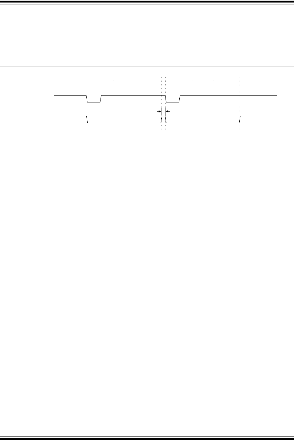
2009-2013 Microchip Technology Inc. DS70000582E-page 39
UART
13.2.5 CLOCK JITTER
Due to jitter or slight frequency differences between devices, it is possible for the next falling bit
edge to be missed for one of the 16x periods. In that case, a one clock wide pulse appears on
the decoded data stream. Since the UART performs a Majority Detect around the bit center, this
does not cause erroneous data (see Figure 13-6 for details).
Figure 13-6: Clock Jitter Causing a Pulse Between Consecutive Zeros
16 Periods 16 Periods
Extra Pulse will be Ignored
UxRX (rx_in)
Decoded Data

dsPIC33/PIC24 Family Reference Manual
DS70000582E-page 40 2009-2013 Microchip Technology Inc.
14.0 LIN/J2602 SUPPORT
The LIN/J2602 protocol transmits data in the form of small blocks, known as frames. Each frame
consists of a Break character with a delimiter, a Sync byte, a protected identifier and the data to
be transmitted (see Figure 14-1).
• Break Sequence: The Break sequence indicates the beginning of a new frame. A Break
sequence generated by the master node consists of a Start bit, followed by twelve bits of ‘0’
and a break delimiter.
• Sync Byte: The Sync is a byte field loaded with the data value of 0x55. When the Auto-
Baud feature is enabled, the UART module uses the Sync byte to compute the baud rate of
the incoming data.
• Protected Identifier: The Protected Identifier contains the identifier and the identifier parity.
Figure 14-1: Frame Structure
14.1 Data Reception Using LIN/J2602 Protocol
When the LIN/J2602 protocol is used, the UART module receives data in the form of frames and
the incoming data is loaded into the receive buffer. For effective data reception, the BRG counter
should be loaded with the baud rate of incoming data.
The bit rate of the incoming data can be detected if the following occurs:
• The auto-baud feature is enabled
• The WAKE bit is set before setting the ABAUD bit
The UART module uses the Sync byte to compute the baud rate of the incoming data. If the
WAKE bit is set before setting the ABAUD bit, the Auto-Baud Rate Detection occurs on the byte
following the Break character. The module receives the Start bit of the Break character, the data
and the invalid Stop bit (which sets FERR), but the receiver waits for a valid Stop bit before receiv-
ing the next Start bit. No further reception can occur until a Stop bit is received. The WAKE bit is
automatically cleared once the Stop bit is received. After the fifth rising edge of the Sync
character is detected, the baud rate of the incoming data is loaded into the BRG counter and the
ABAUD bit is automatically cleared.
If the Auto-Baud feature is enabled without setting the WAKE bit, the delimiter is assumed to be
the first bit of the Sync byte instead of the Start bit. This results in erroneous baud rate calculation.
This happens because the receiver expects a Sync byte at the start of the reception. The LIN/
J2602 protocol, however, initiates the transmission with the Break character and the Sync byte
follows. Thus, the delimiter, which can range from one to four bits, is assumed to be the first low-
to-high transition on the RX line. Therefore, the delimiter acts as a first bit of the Sync byte instead
of the Start bit (see Figure 14-2).
UxRX
bit 0
bit 1
Start
bit 2
bit 3
bit 4
bit 5
bit 6
bit 7
Stop bit
Delimiter
Break Character Sync Byte
Identifier, Data
and Checksum
Note 1: Before data reception, the user application should load the BRG counter of the
UART module with a value approximate to the bit rate of the incoming data.
2: For LIN/J2602 support, the UART error interrupt (caused when FERR is set) may
need to be serviced before the (RX/TX) data interrupts. The UARTx Error Interrupt
Priority Level (UxEIP) must be raised, or the data Interrupt Priority Levels (UxRXIP
and UxTXIP) may be lowered.
Example for UART2 to raise the U2ErrInterrupt level:
• IPC7bits.U2RXIP = 4; //UART2 RX Interrupt Priority, mid-range
• IPC7bits.U2TXIP = 4; //UART2 TX Interrupt Priority, mid-range
• IPC16bits.U2EIP = 5; //UART2 Error Interrupt Priority set higher

2009-2013 Microchip Technology Inc. DS70000582E-page 41
UART
Figure 14-2: Data Reception Using the LIN/J2602 Protocol
BRG
UxRX
bit 0
bit 1
Start
XXXXh 0000h
Edge 1
bit 2
bit 3
Edge 2
bit 4
bit 5
Edge 3
bit 6
bit 7
Edge 4
Stop bit
Edge 5
001Ch
Identifier, Data
and Checksum
Delimiter
Sync Byte
1 6
1. The user application first sets the WAKE bit and then the ABAUD bit.
2. An RX interrupt is generated because the device wakes up on the reception of the Break character.
3. The FERR bit is set.
4. The WAKE bit is cleared.
5. The auto-baud feature detects the first rising edge of the Sync byte.
6. The fifth rising edge of the Sync byte is detected. The ABAUD bit is cleared and the BRG counter is loaded with the
baud rate of the received data.
Auto-Cleared
WAKE bit
ABAUD bit
UxRXIF
52 3 4
Auto-Cleared
Counter
Break Character

dsPIC33/PIC24 Family Reference Manual
DS70000582E-page 42 2009-2013 Microchip Technology Inc.
15.0 SMART CARD SUPPORT
The UART module supports communication with ISO 7816 Smart Cards. In a typical application,
the UART module is intended to act as the master or terminal that always initiates communication
transactions. The Smart Card acts as a slave and always responds to commands and other
stimulus from the terminal. Figure 15-1 shows a Smart Card subsystem using a microcontroller
with a UART module for Smart Card data communication.
The terminal is also responsible for powering, clocking and resetting the Smart Card. The clock
can be sourced by using the REFO output pin and the Reset signal can be implemented with a
general purpose output. The system is based on a half-duplex, single wire requiring that the
UART TX and UART RX pins must be shorted externally and pulled to V
DD with a weak pull-up.
The module can be configured to support either block (T = 1) or byte (T = 0) protocol. Block mode
is set up for a predetermined message block size, whereas Byte mode transmits one byte at a
time.
Upon detection of the card insertion, the terminal pulls the Reset line low to initiate a Reset
sequence. The Smart Card responds with an Answer-To-Reset (ATR), which contains parame-
ters used for communication details. The ATR baud rate is predetermined at REFO clk/372. The
terminal will need to be configured for this baud rate at the time the Reset pulse is sent to the
Smart Card. Typical REFO clock rates are 1 MHz to 5 MHz. See ISO 7816 for additional details
on ATR.
Figure 15-1: Smart Card Subsystem
Note: Some PIC
®
MCU devices have optional built-in support for ISO 7816 Smart Card
communication. Refer to the specific device data sheet for information regarding
Smart Card support.
Te r mi nal
dsPIC33/PIC24
UART
Smart Card
TX
RX
REFO
GPO
GPI
Card Detect
(1)
VDD
GND
V
DD
RST
CLK
I/O
Note 1: Use a general purpose input to detect insertion of a Smart Card.

2009-2013 Microchip Technology Inc. DS70000582E-page 43
UART
15.1 Protocol and Frame Details
The Smart Card communication scheme is based on an Elementary Time Unit (ETU) that is also
the bit clock. The Smart Card will provide the ETU value in the ATR and the terminal is configured
accordingly. A character frame consists of 10 bits; a Start bit, 8 data bits and a parity bit. Depending
on the mode, guard and wait times are used to separate bytes and message transitions.
The ISO 7816 specification defines 2 communication logic conventions: direct and inverse.
Direct convention is defined as LSB first and a high state as logic one. Inverse mode is defined
as MSB first and a low on the line is interpreted as a logic low. The logic convention is set using
the CONV bit (UxSCCON<3>).
15.1.1 GUARD TIME
Guard time is defined as the minimum delay between two consecutive character frames. The
ISO 7816 specification defines both a Character Guard Time (CGT) and a Block Guard Time
(BGT). In both T = 0 and T = 1 modes, CGT is defined as the minimum delay between the leading
edges of the two consecutive characters in the same direction of transmission. Block Guard Time
(BGT) for T = 1 mode only is defined as the minimum delay between the leading edges of the two
consecutive characters in the opposite directions. The BGT has a standard fixed value of 22 ETU.
15.1.2 WAIT TIME
Wait time is the maximum delay allowed between two consecutive characters transmitted by the
card or an interfacing device. The Character Wait Time (CWT) is the maximum delay between
the leading edges of the two consecutive characters in the block, as shown in Figure 15-2. The
minimum delay is CGT. The Block Wait Time (BWT) is the maximum delay between the leading
edge of the last character of the block received by the card and the leading edge of the first
character of the next block transmitted by the card, as shown in Figure 15-3. BWT helps the
interfacing device in detecting the unresponsive Smart Cards. The minimum delay is BGT.
Figure 15-2: Character Guard and Wait Time
Figure 15-3: Block Guard and Wait Time
Note: The guard time count is started after the parity bit is shifted out. The value of the Guard
Time Counter register will have to be calculated to exclude the character frame time.
Note: The LAST bit (UxTXREG<15>) set by user software is used to automatically start
the guard or wait timers, depending on the state of the module.
CGT ≤ t ≤ CWT
Character of a Block Next Character of the Same Block
BGT ≤ t ≤ BWT
Last Character of a Block
First Character of the Next Block
Sent by the Interface Device
Sent by the Card

dsPIC33/PIC24 Family Reference Manual
DS70000582E-page 44 2009-2013 Microchip Technology Inc.
15.1.3 ERROR DETECTION
The transmitter is responsible for calculating the parity bit value. Parity is always even, defined
as the number of logic ones and the parity bit, always being an even count. The receiver also
calculates the parity value and compares it to the received parity bit. If a discrepancy is found,
the error is flagged by the receiver, pulling the line low for a duration defined by T0PD
(UxSCCON<2>).
The transmitter tests the I/O line at Time 11 ± 0.2 ETU after the leading edge of the Start bit of a
character was sent. If the transmitter detects an error by detecting the state low on the I/O line,
it will repeat the disputed character after a delay of at least 2 ETU, following the detection of the
error. The number of repeats is configured with the TXRPT<1:0> bits (UxSCCON<5:4>). See
Figure 15-4 for timing details in T = 0 mode.
Figure 15-4: T = 0 Character Repetition Timing
Note: Protocol characteristics, electrical characteristics of the Smart Card, Answer-To-
Reset (ATR), PPS (Protocol Parameter Selection), calculation of guard time and
wait times are out of scope of this FRM. Please refer to the licensed version of the
ISO 7816-3 document for details about Smart Card communication.
Bit Clock
0 ETU
10.0 ± 0.2 ETU
(2)
10.5 ± 0.2 ETU
(3)
11.0 ± 0.2 ETU
(4)
I/O
Start Bit
Bit 0 Bit 1
(1)
Parity
Note 1: 8-bit character.
2: At 10.0 ± 0.2 ETU, the transmitter disables the driver.
3: At 10.5 ± 0.2 ETU, the receiver sets the I/O line low if a parity error is detected.
4: At 11.0 ± 0.2 ETU, the transmitter tests the I/O line.
5: See T0PD (UxSCCON<2>) in Register 15-1.
Character 1
(5)

2009-2013 Microchip Technology Inc. DS70000582E-page 45
UART
15.2 Smart Card Control Registers
Register 15-1: UxSCCON: UARTx Smart Card Control Register
U-0 U-0 U-0 U-0 U-0 U-0 U-0 U-0
— — — — — — — —
bit 15 bit 8
U-0 U-0 R/W-0 R/W-0 R/W-0 R/W-0 R/W-0 R/W-0
— — TXRPT1
(1)
TXRPT0
(1)
CONV T0PD
(1)
PTRCL SCEN
bit 7 bit 0
Legend:
R = Readable bit W = Writable bit U = Unimplemented bit, read as ‘0’
-n = Value at POR ‘1’ = Bit is set ‘0’ = Bit is cleared x = Bit is unknown
bit 15-6 Unimplemented: Read as ‘0’
bit 5-4 TXRPT<1:0>: Transmit Repeat Selection bits
(1)
11 = Retransmit the error byte four times
10 = Retransmit the error byte three times
01 = Retransmit the error byte twice
00 = Retransmit the error byte once
bit 3 CONV: Logic Convention Selection bit
1 = Inverse logic convention
0 = Direct logic convention
bit 2 T0PD: Pull-Down Duration for T = 0 Error Handling bit
(1)
1 = 2 ETU
0 = 1 ETU
bit 1 PTRCL: Smart Card Protocol Selection bit
1 = T = 1
0 = T = 0
bit 0 SCEN: Smart Card Mode Enable bit
1 = Smart Card mode is enabled if UARTEN (UxMODE<15>) = 1
0 = Smart Card mode is disabled
Note 1: These bits are applicable to T = 0 only. See the PTRCL bit (UxSCCON<1>.

dsPIC33/PIC24 Family Reference Manual
DS70000582E-page 46 2009-2013 Microchip Technology Inc.
Register 15-2: UxSCINT: UARTx Smart Card Interrupt Register
U-0 U-0 R/W-0 R/W-0 U-0 U-0 R/W-0 R/W-0
— — RXRPTIF
(1)
TXRPTIF
(1)
— —WTCIFGTCIF
bit 15 bit 8
U-0 R/W-0 R/W-0 R/W-0 U-0 U-0 R/W-0 R/W-0
— PARIE RXRPTIE TXRPTIE — —WTCIEGTCIE
bit 7 bit 0
Legend:
R = Readable bit W = Writable bit U = Unimplemented bit, read as ‘0’
-n = Value at POR ‘1’ = Bit is set ‘0’ = Bit is cleared x = Bit is unknown
bit 15-14 Unimplemented: Read as ‘0’
bit 13 RXRPTIF: Receive Repeat Interrupt Flag bit
(1)
1 = Parity error has persisted after the same character has been received five times (four retransmits)
0 = Flag is cleared
bit 12 TXRPTIF: Transmit Repeat Interrupt Flag bit
(1)
1 = Line error has been detected after the last retransmit per TXRPT<1:0> (see Register 15-1)
0 = Flag is cleared
bit 11-10 Unimplemented: Read as ‘0’
bit 9 PTRCL: Smart Card Protocol Selection bit
1 = T = 1
0 = T = 0
bit 8 SCEN: Smart Card Mode Enable bit
1 = Smart Card mode is enabled if UARTEN (UxMODE<15>) = 1
0 = Smart Card mode disabled
bit 7 Unimplemented: Read as ‘0’
bit 6 PARIE: Parity Interrupt Enable bit
1 = An interrupt is invoked when a character is received with a parity error; see the PERR bit
(UxSTA<3>) in Register 2-2 for the interrupt flag
0 = Interrupt is disabled
bit 5 RXRPTIE: Receive Repeat Interrupt Enable bit
1 = An interrupt is invoked when a parity error has persisted after the same character has been
received five times (four retransmits)
0 = Interrupt is disabled
bit 4 TXRPTIE: Transmit Repeat Interrupt Enable bit
1 = An interrupt is invoked when line error is detected after the last retransmit, per the TXRPT<1:0>
bits, has been completed (see Register 15-1)
0 = Interrupt is disabled
bit 3-2 Unimplemented: Read as ‘0’
bit 1 WTCIE: Waiting Time Counter Interrupt Enable bit
1 = Waiting Time Counter interrupt is enabled
0 = Waiting Time Counter interrupt is disabled
bit 0 GTCIE: Guard Time Counter Interrupt Enable bit
1 = Guard Time Counter interrupt is enabled
0 = Guard Time Counter interrupt is disabled
Note 1: These bits are applicable to T = 0 only. See the PTRCL bit (UxSCCON<1>.

2009-2013 Microchip Technology Inc. DS70000582E-page 47
UART
Register 15-3: UxGTC: UARTx Guard Time Counter
U-0 U-0 U-0 U-0 U-0 U-0 U-0 R/W-0
— — — — — — —GTC8
bit 15 bit 8
R/W-0 R/W-0 R/W-0 R/W-0 R/W-0 R/W-0 R/W-0 R/W-0
GTC<7:0>
bit 7 bit 0
Legend:
R = Readable bit W = Writable bit U = Unimplemented bit, read as ‘0’
-n = Value at POR ‘1’ = Bit is set ‘0’ = Bit is cleared x = Bit is unknown
bit 15-9 Unimplemented: Read as ‘0’
bit 8-0 GTC<8:0>: Guard Time Counter bits
This counter is operated on the Bit Clock whose period is always equal to one ETU.
Register 15-4: UxWTCL: UARTx Waiting Time Counter (Lower Bits)
R/W-0 R/W-0 R/W-0 R/W-0 R/W-0 R/W-0 R/W-0 R/W-0
WTC<15:8>
bit 15 bit 8
R/W-0 R/W-0 R/W-0 R/W-0 R/W-0 R/W-0 R/W-0 R/W-0
WTC<7:0>
bit 7 bit 0
Legend:
R = Readable bit W = Writable bit U = Unimplemented bit, read as ‘0’
-n = Value at POR ‘1’ = Bit is set ‘0’ = Bit is cleared x = Bit is unknown
bit 8-0 WTC<15:0>: Waiting Time Counter bits
This counter is operated on the Bit Clock whose period is always equal to one ETU.
Register 15-5: UxWTCH: UARTx Waiting Time Counter (Upper Bits)
U-0 U-0 U-0 U-0 U-0 U-0 U-0 U-0
— — — — — — — —
bit 15 bit 8
R/W-0 R/W-0 R/W-0 R/W-0 R/W-0 R/W-0 R/W-0 R/W-0
WTC<23:16>
bit 7 bit 0
Legend:
R = Readable bit W = Writable bit U = Unimplemented bit, read as ‘0’
-n = Value at POR ‘1’ = Bit is set ‘0’ = Bit is cleared x = Bit is unknown
bit 15-8 Unimplemented: Read as ‘0’
bit 7-0 WTC<23:16>: Waiting Time Counter bits
This counter is operated on the Bit Clock whose period is always equal to one ETU.

dsPIC33/PIC24 Family Reference Manual
DS70000582E-page 48 2009-2013 Microchip Technology Inc.
15.3 Smart Card Register Settings
The Smart Card communication protocol features are set using the UxSCCON register and the
Smart Card communication interrupts are set using the UxSCINT register. The guard and waiting
times are set using UxGTC and UxWTCL/UxWTCH registers, respectively, in units of ETU.
15.4 Smart Card Interrupt Configuration
The UART has the ability to generate interrupts reflecting the events that occur during the data
communication with the Smart Card. These interrupts can be controlled using the enable bits in
the UxSCINT register (see Register 15-2). The Smart Card protocol-specific interrupt flag status
bits can be read from the UxSCINT register and should be cleared in software.
Smart Card interrupts should be serviced in the UART error Interrupt Service Routine (ISR).
UART error interrupts must be enabled using the UxERIE bit (IECx<x>). The priority of the UART
error interrupt has to be set using UxERIP bit (IPCx<2:0>).
Example 15-1: Smart Card Interrupt Setup for UART1
15.5 Smart Card Communication
15.5.1 PRE-Answer-To-Reset (ATR) INITIALIZATION
The module should be configured in Receive mode prior to the Reset line being pulled low to
initiate the Smart Card’s response as follows:
1. Write the UxBRG register with a value corresponding to REFO/372.
2. Configure for 8-bit data, even parity, by writing PDSEL<1:0> (UxMODE<2:1>) = 11.
3. Set the SCEN bit (UxSCCON<0>).
4. Set the URXEN bit (UxSTA<12>).
5. Set up and enable the RX interrupt as described in Section 7.3 “Receive Interrupt”.
6. Enable the UART by setting the UARTEN bit (UxMODE<15>).
7. Read data out of UxRXREG as it becomes available and save for ATR processing.
Note: Smart Card bit rate (ETU) is configured by writing the appropriate value to the
UxBRG register.
// Smart card interrupt setup for UART1
U1SCINTbits.GTCIF = 0; // Clear GTC interrupt flag
U1SCINTbits.GTCIE = 1; // Enable guard time count match interrupt
U1SCINTbits.WTCIF = 0; // Clear WTC interrupt flag
U1SCINTbits.WTCIE = 1; // Enable wait time count match interrupt
U1SCINTbits.TXRPTIF = 0; // Clear TX repeat error interrupt flag (Optional)
U1SCINTbits.TXRPTIE = 1; // Enable TX repeat error interrupt (Optional)
U1SCINTbits.RXRPTIF = 0; // Clear TX repeat error interrupt flag (Optional)
U1SCINTbits.RXRPTIE = 1; // Enable RX repeat error interrupt (Optional)
U1STAbits.PERR = 0; // Clear Parity error flag (Optional)
U1SCINTbits.PARIE = 1; // Enable RX parity error interrupt (Optional)
// UART 1 Error interrupt
IPC16bits.U1ERIP = 5; // Error interrupt priority
IFS4bits.U1ERIF = 0; // Clear U1 error flag
IEC4bits.U1ERIE = 1; // Enable error interrupts

2009-2013 Microchip Technology Inc. DS70000582E-page 49
UART
15.5.2 POST-Answer-To-Reset (ATR) INITIALIZATION
After the terminal has done a reset of the Smart Card and received the setup parameters
contained in the ATR, the user software can configure the module for communication as follows:
1. Disable the UART for configuration changes by clearing the UARTEN bit.
2. Set the PTRCL (UxSCCON<1>), T0PD (UxSCCON<2>), CONV (UxSCCON<3>) and
TXRPT<1:0> bits (UxSCCON<5:4>) according to ATR parameters.
3. Program the UxBRG register for the ETU defined in ATR.
4. Program the UxGTC register and set GTCIE (UxSCINT<0>).
5. Program UxWTCL/H registers and set WTCIE (UxSCINT<1>).
6. Enable interrupts as described in Section 7.3 “Receive Interrupt”, Section 15.2 “Smart
Card Control Registers” and Section 15.4 “Smart Card Interrupt Configuration”.
7. Clear the URXEN bit.
8. Enable the UART by setting the UARTEN bit.
9. Set the UTXEN bit (UxSTA<10>) to start the first transmission to the Smart Card.
Example 15-2: Smart Card Initialization Code for UART1
15.5.3 T = 0 PROTOCOL COMMUNICATION
Transmission with T = 0:
1. Set URXEN to ‘0’ and UTXEN to ‘1’.
2. Write data into UxTXREG.
3. Take appropriate actions according to the ISO 7816 standard if the WTCIF, GTCIF and/or
TXRPTIF bits are set.
4. Set LAST = 1 (UxTXREG<15>) for the last byte of data.
Reception with T =
0:
1. Set UTXEN to ‘0’ and URXEN to ‘1’.
2. Read the UxRXREG as the data becomes available upon the receive interrupt.
3. Take appropriate actions according to the ISO 7816 standard if the WTCIF, GTCIF and/or
RXRPTIF bits are set.
Note: Only one enable bit (UTXEN or URXEN) can be set at any given time.
// Smart card initialization code example for UART1
U1BRG = 25; // Set bit rate
U1MODEbits.PDSEL = 0x01; // 8 bits, even parity
// Smart card specific register configuration
U1SCCONbits.SCEN = 1; // Enable Smart card mode
U1SCCONbits.PTRCL = 0; // T=0 protocol
U1SCCONbits.T0PD = 0; // 1 ETU pull down duration
U1SCCONbits.CONV = 0; // Direct logic convention
U1SCCONbits.TXRPT = 1; // Retransmit error byte 2 times
U1GTC = 0x0012; // Guard time = 12 ETU
U1WTCL = 0x0022; // Wait time = 22 ETU
U1WTCH = 0x0000;
U1MODEbits.UARTEN = 1; // Enable UART
Note: Due to the TX and RX pins being shorted, a receive interrupt will be generated on
transmission of a character, if enabled. It is recommended to disable receive
interrupts when transmitting.
Note: For the last character, the user must ensure that the guard time is satisfied before
transmitting the response. The GTC may be used for this purpose, whereas the
WTC interrupt may be disabled or ignored.

dsPIC33/PIC24 Family Reference Manual
DS70000582E-page 50 2009-2013 Microchip Technology Inc.
15.5.4 T = 1 PROTOCOL COMMUNICATION
Transmission with T = 1:
1. Set URXEN to ‘0’ and UTXEN to ‘1’.
2. Write data into UxTXREG.
3. Program the value of BWT to UxWTCL/H and set WTCIE (UxSCINT<1>) to ‘1’.
4. Take appropriate actions according to the ISO 7816 standard if the WTCIF, GTCIF and/or
TXRPTIF bits are set.
5. Set the LAST = 1 bit (UxTXREG<15>) for the last byte of data.
Reception with T = 1:
1. Set UTXEN to ‘0’ and URXEN to ‘1’.
2. Read the UxRXREG as the data becomes available upon the receive interrupt.
3. Program the value of CWT to UxWTCL/H and set WTCIE (UxSCINT<1>) to ‘1’.
4. Take appropriate actions according to the ISO 7816 standard if the WTCIF, GTCIF and/or
RXRPTIF bits are set.
Note: For the last character, the user must ensure the guard time is satisfied before trans-
mitting the response. The GTC may be used for this purpose, whereas the WTC
interrupt may be disabled or ignored.

2009-2013 Microchip Technology Inc. DS70000582E-page 51
UART
16.0 REGISTERS MAP
A summary of the registers associated with the UART module of the dsPIC33 and PIC24 device families is provided in Tab le 1 6 -1 .
Table 16-1: Registers Associated with UARTx
(1)
SFR Name Bit 15 Bit 14 Bit 13 Bit 12 Bit 11 Bit 10 Bit 9 Bit 8 Bit 7 Bit 6 Bit 5 Bit 4 Bit 3 Bit 2 Bit 1 Bit 0
All
Resets
UxMODE UARTEN — USIDL IREN RTSMD ALTIO UEN1 UEN0 WAKE LPBACK ABAUD URXINV BRGH PDSEL1 PDSEL0 STSEL
0000
UxSTA UTXISEL1 UTXINV UTXISEL0 URXEN UTXBRK UTXEN UTXBF TRMT URXISEL1 URXISEL0 ADDEN RIDLE PERR FERR OERR URXDA
0110
UxADMD ADM_MASK7 ADM_MASK6 ADM_MASK5 ADM_MASK4 ADM_MASK3 ADM_MASK2 ADM_MASK1 ADM_MASK0 ADM_ADDR7 ADM_ADDR6 ADM_ADDR5 ADM_ADDR4 ADM_ADDR3 ADM_ADDR2 ADM_ADDR1 ADM_ADDR0
0000
UxTXREG LAST — — — — — — UTX8 UARTx Transmit Register
xxxx
UxRXREG — — — — — — — URX8 UARTx Receive Register
0000
UxBRG Baud Rate Generator Prescaler Register
0000
UxSCCON — — — — — — — — — —TXRPT1
(2)
TXRPT0
(2)
CONV T0PD
(2)
PTRCL SCEN
0000
UxSCINT — —RXRPTIF
(2)
TXRPTIF
(2)
— —WTCIFGTCIF — PARIE RXRPTIE TXRPTIE — —WTCIEGTCIE
0000
UxGTC — — — — — — — GTC8 GTC7 GTC6 GTC5 GTC4 GTC3 GTC2 GTC1 GTC0
0000
UxWTCL WTC15 WTC14 WTC13 WTC12 WTC11 WTC10 WTC9 WTC8 WTC7 WTC6 WTC5 WTC4 WTC3 WTC2 WTC1 WTC0
0000
UxWTCH — — — — — — — — WTC23 WTC22 WTC21 WTC20 WTC19 WTC18 WTC17 WTC16
0000
Legend:
x
= unknown value on Reset, — = unimplemented, read as ‘
0
’. Reset values are shown in hexadecimal.
Note 1:
The registers associated with UARTx are shown for reference. Refer to the
“Universal Asynchronous Receiver Transmitter (UART)”
chapter of the specific device data sheet for the registers associated with other UART modules.
2:
These bits are applicable to T =
0
only. See the PTRCL bit (UxSCCON<1>).

dsPIC33/PIC24 Family Reference Manual
DS70000582E-page 52 2009-2013 Microchip Technology Inc.
17.0 RELATED APPLICATION NOTES
This section lists application notes that are related to this section of the manual. These applica-
tion notes may not be written specifically for the dsPIC33 and PIC24 device families, but the
concepts are pertinent and could be used with modification and possible limitations. The current
application notes related to the UART module include the following:
Title Application Note #
Smart Card Communication Using PIC
®
MCUs AN1370
Note: Please visit the Microchip web site (www.microchip.com) for additional application
notes and code examples for the dsPIC33 and PIC24 families of devices.

2009-2013 Microchip Technology Inc. DS70000582E-page 53
UART
18.0 REVISION HISTORY
Revision A (January 2009)
This is the initial released version of the document.
Revision B (July 2010)
This revision includes the following changes:
• Changed the document name from dsPIC33E Family Reference Manual to dsPIC33E/
PIC24E Family Reference Manual
• Deleted watermark from the code examples
• Added Note 3 in the note box in Section 11.2 “UART Operation in Idle Mode”
• Updated and added a note to Figure 7-2
• Updated Figure 8-1
• Added Figure 10-1
• Changed the bit 8 characteristic from W-x to R/W-0 in Register 2-6
• Minor changes to the text and formatting have been incorporated throughout the document
Revision C (December 2011)
This revision includes the following updates:
• Updated the baud rate feature values and the hardware flow control option in Section 1.0
“Introduction”
• Relocated the note box originally located in 17.1 “Introduction” to Section 2.0 “Control
Registers”
• Changed all occurrences of the instruction cycle clock frequency (F
CY) to: FP
• Changed all occurrences of Low-Speed mode to: Standard-Speed mode
• Added Note 2 and updated the bit value definitions for BRGH in UxMODE: UARTx Mode
Register (see Register 2-1)
• Updated the UART Transmission with Interrupts (see Example 5-1)
• Updated the UART Receive Only with Polling (Interrupts Disabled) (see Example 7-1)
• Updated the UART Reception and Transmission with DMA (see Example 7-1)
• Added a note box to Section 12.0 “Operation of UxCTS and UxRTS Control Pins”
• Removed 17.16 “Design Tips”
• Minor updates to text and formatting were incorporated throughout the document
Revision D (April 2012)
This revision includes the following updates:
• Added a note to Section 7.0 “UART Receiver”
• Added a note to Section 14.0 “LIN/J2602 Support”
• Additional minor updates to text and formatting were incorporated throughout the document
Revision E (October 2013)
This revision includes the following updates:
• Name of Family Reference Manual has been changed to “dsPIC33/PIC24 Family
Reference Manual”
• Section number has been removed from the title
• Side tabs with section numbers have been removed
• Added Smart Card Communication section
• Additional minor updates to text and formatting were incorporated throughout the document

dsPIC33/PIC24 Family Reference Manual
DS70000582E-page 54 2009-2013 Microchip Technology Inc.
NOTES:

2009-2013 Microchip Technology Inc. DS70000582E-page 55
Information contained in this publication regarding device
applications and the like is provided only for your convenience
and may be superseded by updates. It is your responsibility to
ensure that your application meets with your specifications.
MICROCHIP MAKES NO REPRESENTATIONS OR
WARRANTIES OF ANY KIND WHETHER EXPRESS OR
IMPLIED, WRITTEN OR ORAL, STATUTORY OR
OTHERWISE, RELATED TO THE INFORMATION,
INCLUDING BUT NOT LIMITED TO ITS CONDITION,
QUALITY, PERFORMANCE, MERCHANTABILITY OR
FITNESS FOR PURPOSE. Microchip disclaims all liability
arising from this information and its use. Use of Microchip
devices in life support and/or safety applications is entirely at
the buyer’s risk, and the buyer agrees to defend, indemnify and
hold harmless Microchip from any and all damages, claims,
suits, or expenses resulting from such use. No licenses are
conveyed, implicitly or otherwise, under any Microchip
intellectual property rights.
Trademarks
The Microchip name and logo, the Microchip logo, dsPIC,
FlashFlex, K
EELOQ, KEELOQ logo, MPLAB, PIC, PICmicro,
PICSTART, PIC
32
logo, rfPIC, SST, SST Logo, SuperFlash
and UNI/O are registered trademarks of Microchip Technology
Incorporated in the U.S.A. and other countries.
FilterLab, Hampshire, HI-TECH C, Linear Active Thermistor,
MTP, SEEVAL and The Embedded Control Solutions
Company are registered trademarks of Microchip Technology
Incorporated in the U.S.A.
Silicon Storage Technology is a registered trademark of
Microchip Technology Inc. in other countries.
Analog-for-the-Digital Age, Application Maestro, BodyCom,
chipKIT, chipKIT logo, CodeGuard, dsPICDEM,
dsPICDEM.net, dsPICworks, dsSPEAK, ECAN,
ECONOMONITOR, FanSense, HI-TIDE, In-Circuit Serial
Programming, ICSP, Mindi, MiWi, MPASM, MPF, MPLAB
Certified logo, MPLIB, MPLINK, mTouch, Omniscient Code
Generation, PICC, PICC-18, PICDEM, PICDEM.net, PICkit,
PICtail, REAL ICE, rfLAB, Select Mode, SQI, Serial Quad I/O,
Total Endurance, TSHARC, UniWinDriver, WiperLock, ZENA
and Z-Scale are trademarks of Microchip Technology
Incorporated in the U.S.A. and other countries.
SQTP is a service mark of Microchip Technology Incorporated
in the U.S.A.
GestIC and ULPP are registered trademarks of Microchip
Technology Germany II GmbH & Co. KG, a subsidiary of
Microchip Technology Inc., in other countries.
All other trademarks mentioned herein are property of their
respective companies.
© 2009-2013, Microchip Technology Incorporated, Printed in
the U.S.A., All Rights Reserved.
Printed on recycled paper.
ISBN: 978-1-62077-507-3
Note the following details of the code protection feature on Microchip devices:
• Microchip products meet the specification contained in their particular Microchip Data Sheet.
• Microchip believes that its family of products is one of the most secure families of its kind on the market today, when used in the
intended manner and under normal conditions.
• There are dishonest and possibly illegal methods used to breach the code protection feature. All of these methods, to our
knowledge, require using the Microchip products in a manner outside the operating specifications contained in Microchip’s Data
Sheets. Most likely, the person doing so is engaged in theft of intellectual property.
• Microchip is willing to work with the customer who is concerned about the integrity of their code.
• Neither Microchip nor any other semiconductor manufacturer can guarantee the security of their code. Code protection does not
mean that we are guaranteeing the product as “unbreakable.”
Code protection is constantly evolving. We at Microchip are committed to continuously improving the code protection features of our
products. Attempts to break Microchip’s code protection feature may be a violation of the Digital Millennium Copyright Act. If such acts
allow unauthorized access to your software or other copyrighted work, you may have a right to sue for relief under that Act.
Microchip received ISO/TS-16949:2009 certification for its worldwide
headquarters, design and wafer fabrication facilities in Chandler and
Tempe, Arizona; Gresham, Oregon and design centers in California
and India. The Company’s quality system processes and procedures
are for its PIC
®
MCUs and dsPIC
®
DSCs, KEELOQ
®
code hopping
devices, Serial EEPROMs, microperipherals, nonvolatile memory and
analog products. In addition, Microchip’s quality system for the design
and manufacture of development systems is ISO 9001:2000 certified.
QUALITY MANAGEMENT S
YSTEM
CERTIFIED BY DNV
== ISO/TS 16949 ==

DS70000582E-page 56 2009-2013 Microchip Technology Inc.
AMERICAS
Corporate Office
2355 West Chandler Blvd.
Chandler, AZ 85224-6199
Tel: 480-792-7200
Fax: 480-792-7277
Technical Support:
http://www.microchip.com/
support
Web Address:
www.microchip.com
Atlanta
Duluth, GA
Tel: 678-957-9614
Fax: 678-957-1455
Boston
Westborough, MA
Tel: 774-760-0087
Fax: 774-760-0088
Chicago
Itasca, IL
Tel: 630-285-0071
Fax: 630-285-0075
Cleveland
Independence, OH
Tel: 216-447-0464
Fax: 216-447-0643
Dallas
Addison, TX
Tel: 972-818-7423
Fax: 972-818-2924
Detroit
Farmington Hills, MI
Tel: 248-538-2250
Fax: 248-538-2260
Indianapolis
Noblesville, IN
Tel: 317-773-8323
Fax: 317-773-5453
Los Angeles
Mission Viejo, CA
Tel: 949-462-9523
Fax: 949-462-9608
Santa Clara
Santa Clara, CA
Tel: 408-961-6444
Fax: 408-961-6445
Toronto
Mississauga, Ontario,
Canada
Tel: 905-673-0699
Fax: 905-673-6509
ASIA/PACIFIC
Asia Pacific Office
Suites 3707-14, 37th Floor
Tower 6, The Gateway
Harbour City, Kowloon
Hong Kong
Tel: 852-2401-1200
Fax: 852-2401-3431
Australia - Sydney
Tel: 61-2-9868-6733
Fax: 61-2-9868-6755
China - Beijing
Tel: 86-10-8569-7000
Fax: 86-10-8528-2104
China - Chengdu
Tel: 86-28-8665-5511
Fax: 86-28-8665-7889
China - Chongqing
Tel: 86-23-8980-9588
Fax: 86-23-8980-9500
China - Hangzhou
Tel: 86-571-2819-3187
Fax: 86-571-2819-3189
China - Hong Kong SAR
Tel: 852-2943-5100
Fax: 852-2401-3431
China - Nanjing
Tel: 86-25-8473-2460
Fax: 86-25-8473-2470
China - Qingdao
Tel: 86-532-8502-7355
Fax: 86-532-8502-7205
China - Shanghai
Tel: 86-21-5407-5533
Fax: 86-21-5407-5066
China - Shenyang
Tel: 86-24-2334-2829
Fax: 86-24-2334-2393
China - Shenzhen
Tel: 86-755-8864-2200
Fax: 86-755-8203-1760
China - Wuhan
Tel: 86-27-5980-5300
Fax: 86-27-5980-5118
China - Xian
Tel: 86-29-8833-7252
Fax: 86-29-8833-7256
China - Xiamen
Tel: 86-592-2388138
Fax: 86-592-2388130
China - Zhuhai
Tel: 86-756-3210040
Fax: 86-756-3210049
ASIA/PACIFIC
India - Bangalore
Tel: 91-80-3090-4444
Fax: 91-80-3090-4123
India - New Delhi
Tel: 91-11-4160-8631
Fax: 91-11-4160-8632
India - Pune
Tel: 91-20-3019-1500
Japan - Osaka
Tel: 81-6-6152-7160
Fax: 81-6-6152-9310
Japan - Tokyo
Tel: 81-3-6880- 3770
Fax: 81-3-6880-3771
Korea - Daegu
Tel: 82-53-744-4301
Fax: 82-53-744-4302
Korea - Seoul
Tel: 82-2-554-7200
Fax: 82-2-558-5932 or
82-2-558-5934
Malaysia - Kuala Lumpur
Tel: 60-3-6201-9857
Fax: 60-3-6201-9859
Malaysia - Penang
Tel: 60-4-227-8870
Fax: 60-4-227-4068
Philippines - Manila
Tel: 63-2-634-9065
Fax: 63-2-634-9069
Singapore
Tel: 65-6334-8870
Fax: 65-6334-8850
Taiwan - Hsin Chu
Tel: 886-3-5778-366
Fax: 886-3-5770-955
Taiwan - Kaohsiung
Tel: 886-7-213-7828
Fax: 886-7-330-9305
Taiwan - Taipei
Tel: 886-2-2508-8600
Fax: 886-2-2508-0102
Thailand - Bangkok
Tel: 66-2-694-1351
Fax: 66-2-694-1350
EUROPE
Austria - Wels
Tel: 43-7242-2244-39
Fax: 43-7242-2244-393
Denmark - Copenhagen
Tel: 45-4450-2828
Fax: 45-4485-2829
France - Paris
Tel: 33-1-69-53-63-20
Fax: 33-1-69-30-90-79
Germany - Munich
Tel: 49-89-627-144-0
Fax: 49-89-627-144-44
Italy - Milan
Tel: 39-0331-742611
Fax: 39-0331-466781
Netherlands - Drunen
Tel: 31-416-690399
Fax: 31-416-690340
Spain - Madrid
Tel: 34-91-708-08-90
Fax: 34-91-708-08-91
UK - Wokingham
Tel: 44-118-921-5869
Fax: 44-118-921-5820
Worldwide Sales and Service
08/20/13
